Introduction
As it becomes increasingly difficult to scale devices down to improve performance, alternate approaches such as 3D chip stacks are being developed, which improve system performance by increasing the interconnect density and reducing the interconnect length(1). The stacking of multiple chips with through silicon vias (TSV) and fine pitch microbumps between them not only increases the bandwidth and reduces the latency between the chips, but it also increases the difficulty of adequately cooling the devices during operation.

With a conventional lid-less chip package, Fig. 1(a), the thermal path from the active circuits is through the silicon substrate, which can act as a heat spreader, and through the thermal interface material (TIM) layer to the heat sink. Typically, only a small fraction of the heat flows through the back-end-of-line (BEOL) wiring layers on the chip and the solder bumps into the package substrate. With a 3D chip stack, the heat from multiple chips is now being removed through the back surface of the top chip and both the BEOL wiring layers and the microbump layer between chips are in the thermal path, Fig. 1(b). Additionally, the chips that contain TSVs are thinned so that they are less effective at spreading heat from hot spots.
To be able to design systems based on 3D chip stacks, it is necessary to accurately characterize the additional thermal resistance from the BEOL and the microbump layers between chips. There have been extensive theoretical studies of the thermal resistance in 3D chip stacks(2-6), but only limited experimental measurements have been reported(7-9). In previous work(10), we reported on thermal resistance measurements in 4-layer chip stacks with ~25 μm diameter Pb-free solder microbumps with pitches of 50, 71, and 100 μm both with and without underfill.
Thermal Chip Stack Design and Testing
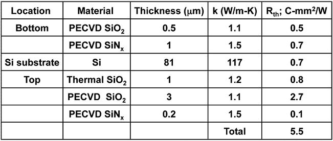
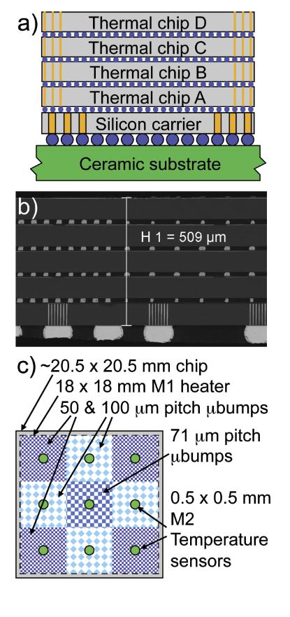
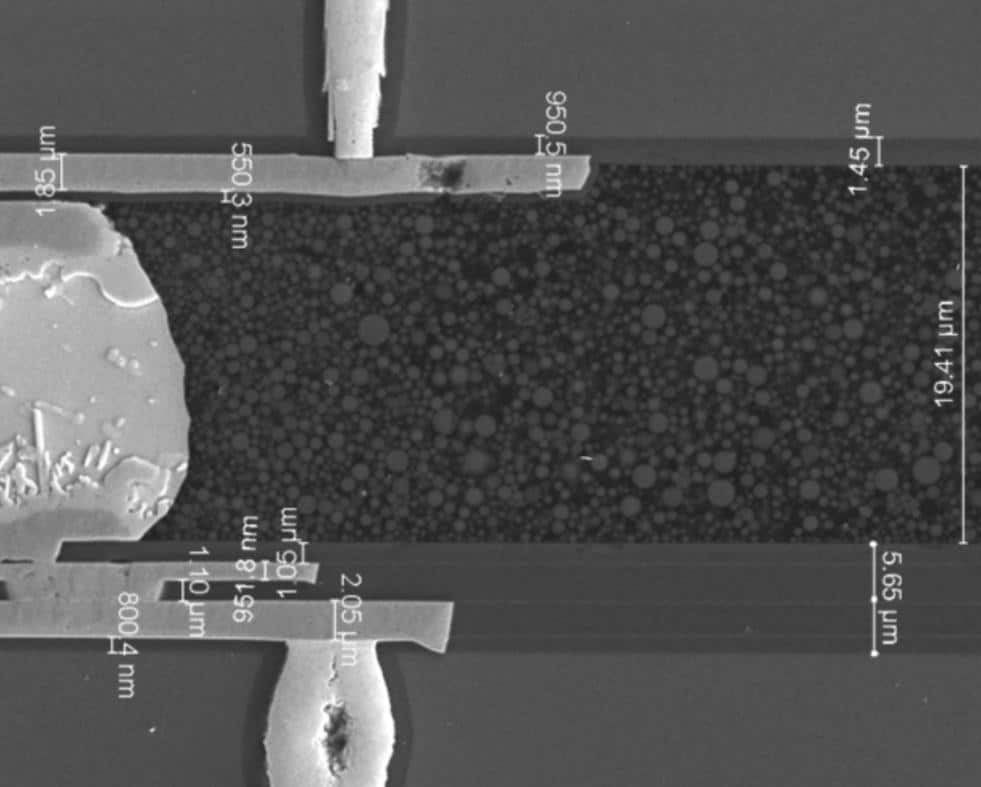
The design of the thermal chip stack test vehicle is described in Fig. 2. The test vehicle consists of a ceramic substrate, a silicon carrier, and four thermal chips, shown schematically in Fig. 2(a). A cross-sectional image of an assembled thermal chip stack is shown in Fig. 2(b). The thermal chip, M1 heater, and M2 resistive temperature sensors dimensions are shown in Fig. 2(c). The thermal chips were joined together with ~ 25 μm diameter Pb-free solder microbumps, which had an average height of 16 μm after bonding. The underfill material used had a measured thermal conductivity of 0.55 W/m-K. The region above the heater was divided into nine 6 x 6 mm areas where the microbump pitch was 50 μm in the corner areas, 100 μm in the areas located along the center of each side, and 71 μm in the center area; see Fig. 2(c). The resistive temperature sensors were centered in each of these areas and were aligned above each other in the chip stack. As shown in Fig. 2(a), there were no TSVs through the thermal chips in the central area where the heater was located; the electrical connections between layers were all in the perimeter region. In addition to the silicon, a number of insulator layers were present on the top and bottom surfaces of the chips and in the thermal measurement region, see Fig. 3. The composition, thickness, and unit thermal resistance values are listed in Table 1. The unit thermal resistance through the chip is approximately 5.5 C-mm2/W (10) .
The thermal chip stack was characterized in a test station where the substrate was clamped to a hybrid LGA (land grid array) socket on a test card and a water cooled cold plate was coupled to the top of the chip stack by using a removable TIM material. The temperature of the water circulating through the cold plate was controlled by a recirculation chiller and monitored by the data acquisition system. Four-point resistance measurements were performed on all the resistive temperature sensors and a constant current source was used to power the heater. The sensor resistors were all individually calibrated by varying the water temperature, measuring the sensor resistor values, and performing a least-square-fit to the resulting data. The uncertainty in the measured thermal resistance is < 5% for the 50 μm pitch and < 10% for the 100 μm pitch regions and is mainly due to uncertainty in the sensor calibration and heat flowing into the substrate or spreading laterally rather than through the chip stack to the cold plate.
Results & Discussion
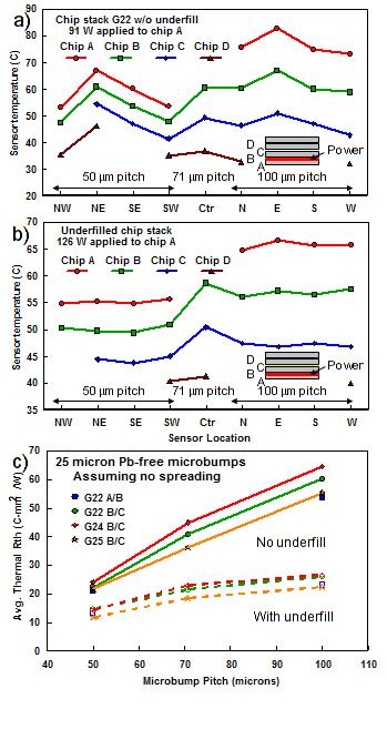
Results are shown in Fig. 4 for the chip stack, sample number G22, before underfill (a) and after underfill was applied (b). Power was supplied to the heater of the bottom chip of the stack (chip A, see Fig. 2a) and the temperate values were measured at the various temperature sensors in the chip stack. In Fig. 4(a,b), the sensor locations and microbump pitch are indicated on the x-axis, where NW, NE, etc refer to different areas of the chip. As would be expected, the chips lower down in the stack, i.e. further from the heat sink, are hotter. For the chip stack without underfill, the higher temperatures in area NE versus the other 50 micron pitch areas is believed to be due to variations in the thickness of the TIM layer between the chip stack and coldplate. Note that the temperature difference between adjacent chips increases as the pitch of the microbumps is increased. The temperature difference between chips is not directly comparable between the results without underfill and with underfill as the power applied was different.
The measured unit thermal resistance of ~25 μm diameter Pb-free microbumps with a pitch of 50 μm, 71 μm, and 100 μm both with and without underfill is plotted in Fig. 4(c). These results are from three thermal chip stacks, sample numbers G22, G24 & G25. For the 50 μm and 100 μm pitch areas, the results are only reported when three or four aligned sensor pairs are available across the specific microbump layer. For the 71 μm pitch area, only one sensor pair is available for each microbump layer. The unit thermal resistance values were calculated assuming no thermal spreading;
Unit Thermal Rth = DTadjacent layers * AreaHeater / Power (1)
Note that the values plotted in Fig. 4(c) include the thermal resistance of ~ 5.5 C-mm2/W from the thermal chip. For the underfilled case, if we subtract the contribution from the thermal chip from the average values, for microbump pitches of 50, 71, and 100 μm, the corresponding unit thermal resistances values are 8.0, 15.5, and 19.0 C-mm2/W.
The chip stack was modeled using commercially available thermal simulation software. A conduction model was used which included all components of the package and board. The silicon die and carrier were given default temperature dependent silicon properties and the insulator layers in table 1 were included. Each of the microbump regions were modeled as homogeneous collapsed cuboids, with effective thru-plane thermal conductivities using a parallel thermal resistance approximation of solder (k = 35 W/m-k), and air or underfill;
keff = ksolder * (fraction solder) + k air * (fraction air or underfill) (2)
Heat transfer coefficient boundary conditions were used to simulate the water cooling and board heat losses. The heat transfer boundary conditions on the bottom of the board were varied from 0 W/m2-K (completely insulated) to 20 W/m2-K to try and determine whether spreading or heat loss through the board was contributing to different resistance values at different layers. We found that the difference in results from varying the heat loss to the board were insignificant and could not explain the differences in resistances at different layers. The spreading was found to be the dominant factor.
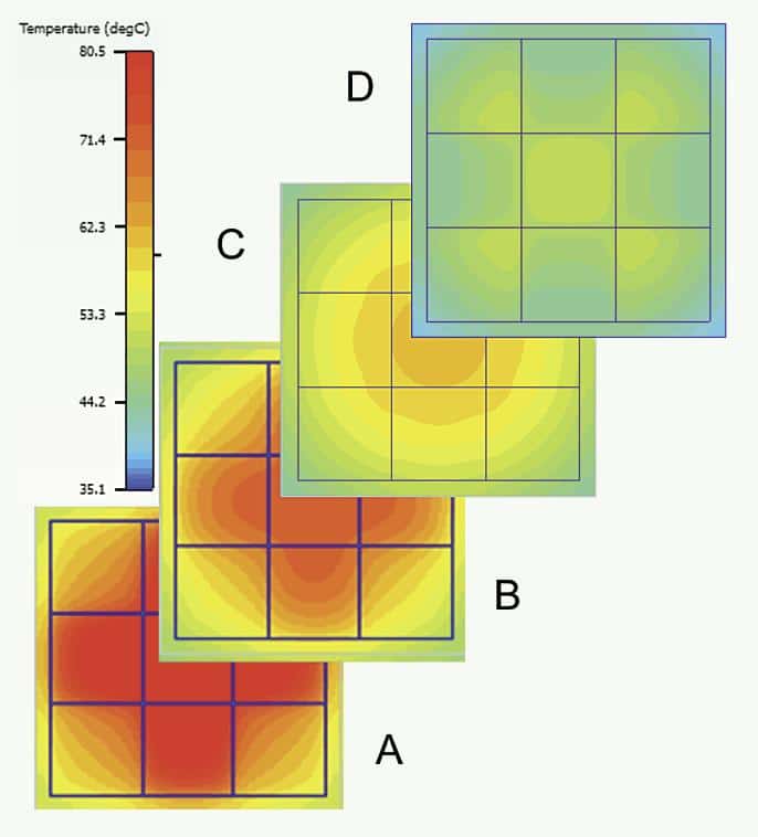
The modeled temperature contours, when the bottom chip A was powered are shown in Fig. 5 for the four high chip stack without underfill. The systematic temperature variations in Fig. 5 are roughly consistent with the measured values plotted in Fig. 4(a,b). At the bottom of the chip stack (chips A & B) the hottest areas are those with the 71 μm and 100 μm pitch microbumps and the temperature distribution is more uniform at the top of the chip stack (chips C & D).
This microbump layer unit thermal resistance includes the contribution from the BLM (ball limiting metallurgy) layers on the chips and intermetallic formation in the Pb-free solder microbumps. The measured values are higher than parallel/series estimates using bulk conductivity values for the solder and underfill. This can be explained by material interfacial resistances, voids, and grain boundary effects. For comparison, with a typical underfilled C4 layer with 200 μm pitch and about 70 μm height, the comparable thermal resistance value is about 100 C-mm2/W. For the 50 μm pitch case, if the unit thermal resistance of the microbump layer is assumed to be from two thermal resistance terms in parallel, where the value measured without underfill corresponds to the thermal resistance of the microbumps alone, then the thermal conductance of the underfill can be estimated to be roughly equal to that of the microbumps alone. This estimation ignores the spreading resistance term and the conduction through air in the no underfill case.
Conclusions
The thermal resistance of Pb-free ~25 μm diameter microbumps with pitches of 50, 71, and 100 μm has been measured with and without underfill in four-layer chip stacks. With underfill, the unit thermal resistance values were 8.0, 15.5, and 19.0 C-mm2/W for 50, 71, and 100 μm pitch microbumps, respectively. For the 50 μm pitch case, the thermal conduction from the underfill is roughly equal to that of the microbumps alone. In this work, we have experimentally characterized the thermal resistance of Pb-free microbumps in a chip stack, which is necessary for the design of future systems based on 3D chip stacks.
Acknowledgments
We are deeply indebted to P. Andry, B. Dang, J.H. Magerlein, J. Maria, and R. Polastre for their assistance with this work.
References
- Knickerbocker, J. U., Andry, P. S., Dang, B., Horton, R. R., Interrante, M. J., Patel, C. S., Polastre, R. J., Sakuma, K., Sirdeshmukh, R., Sprogis, E. J., Sri-Jayantha, S. M., Stephens, A. M., Topol, A. W., Tsang, C. K., Webb, B. C., Wright, S. L., “Three-Dimensional Silicon Integration”, IBM Journal of Research and Development , Vol. 52, No. 6, pp. 553-569, 2008.
- Black, B., Annavaram, M., Brekelbaum, N., DeVale, J., Jiang, L., Loh, G.H., McCaule, D., Morrow, P., Nelson, D.W., Pantuso, D., Reed, P., Rupley, J., Shankar, S., Shen, J., Webb, C., “Die Stacking (3D) Microarchitecture”, Proc. of 39th IEEE/ACM International Symposium on Microarchitecture, MICRO-39, pp. 469-479, 2006.
- Leduca, P., de Crecy, F., Fayolle, M., Charlet, B., Enot, T., Zussy, M., Jones, B., Barbe, J.-C., Kernevez, N., Sillon, N., Maitrejean, S., Louisa, D., “Challenges for 3D IC Integration: Bonding Quality and Thermal Management”, Proc. of IEEE International Interconnect Technology Conference, pp. 210-212, 2007.
- Agonafer, D., Kaisare, A., Hossain, M., Lee, Y., Dewan-Sandur, B., Dishongh, T., Pekin, S., “Thermo-Mechanical Challenges in Stacked Packaging”, Heat Transfer Engineering, Vol. 29, No. 2, pp. 134-148, 2008.
- Jain, A., Jones, R.E., Chatterjee, R., Pozder, S., “Analytical and Numerical Modeling of the Thermal Performance of Three-Dimensional Integrated Circuits”, IEEE Transactions on Components and Packaging Technologies, Vol. 33, No.1, pp. 56-63, 2010.
- Wakil, J., Colgan, E. G., Chen, S., “Back-End-of-Line and Micro-C4 Thermal Resistance Contributions to 3-D Stack Packages”, IEEE Transactions on Components, Packaging and Manufacturing Technology, Vol. 1, No. 7, pp. 1007-1014, 2011.
- Matsumoto, K., Ibaraki, S., Sueoka, K., Sakuma, K., Kikuchi, H., Orii, Y., Yamada, F., “Experimental Thermal Resistance Evaluation of a Three-Dimensional (3D) Chip Stack”, Proc. of 27th IEEE Semiconductor Thermal Measurement and Management Symposium (SEMI-THERM), pp. 125-130, 2011.
- Matsumoto, K., Ibaraki, S., Sueoka, K., Sakuma, K., Kikuchi, H., Orii, Y., Yamada, F., “Experimental Thermal Resistance Evaluation of a Three-Dimensional (3D) Chip Stack, Including Transient Measurements”, Proc. of 28th IEEE Semiconductor Thermal Measurement and Management Symposium (SEMI-THERM), pp. 8-13, 2012.
- Oprins, H., Cherman, V., Vandevelde, B., Torregiani, C., Stucchi, M., Van der Plas, G., Marchal, P., Beyne, E., “Characterization of the Thermal Impact of Cu-Cu Bonds Achieved using TSVs on Hot Spot Dissipation in 3D Stacked ICs”, Proc. 61st IEEE Electronic Components and Technology Conference (ECTC), pp. 861-868, 2011.
- Colgan, E.G., Andry, P., Dang, B., Magerlein, J.H., Maria, J., Polastre, R.J., Wakil, J., “Measurement of microbump thermal resistance in 3D chip stacks,” Proc. of 28th Semiconductor Thermal Measurement and Management Symposium (SEMI-THERM), pp.1-7, 2012.
Evan G. Colgan received a BS in Applied Physics from Caltech in 1982 and a PhD in Materials Science from Cornell in 1987. Dr. Colgan joined IBM in 1987 and worked on silicides, selective CVD-W, diffusion barriers, and both Cu- and Al-based chip wiring. He transferred to IBM Research as a Research Staff Member in 1995 to manage the TFT processing dept, and subsequently worked on a number of display related projects. He joined the packaging area in 2001 and has worked on optical packaging, high performance liquid cooling including silicon microchannels, super computer packaging, and 3D chip stacks. Dr. Colgan has over 100 technical publications, 122 issued US patents, and is a member of APS, MRS, and a Senior Member of IEEE.
Jamil A. Wakil is currently working on data center thermal development for IBM systems, focusing on water cooling and energy efficiency. He joined the IBM Microelectronics packaging group in 1999, where he spent ten years on first level thermal development of organic packages and 3D stack packages. He holds an MS and Ph.D. in mechanical engineering from The University of Texas at Austin, a B.S. in mechanical engineering from Texas A&M University at College Station, and a B.S. in Electrical engineering from the University of Texas at Dallas. Jamil has eight patents and several refereed publications.


