Jason Carter, Jeremy Acord, Dan Hoffmann, Andrew Trageser, Charles Pagel
Penn State University – Electro-Optics Center, Freeport, Pa.NSWC, Crane Division, Crane, Ind.
1. Introduction
As a nascent technology compared to GaAs, Si, or nonsolid state technology, GaN-on-SiC transistors have not established a history of reliability from which end-users of the technology can establish its long term replacement and refurbishment costs [1]. Nonetheless, GaN provides a number of distinct advantages over older technologies, including improved heat transfer properties, wider bandgap energy, higher operational temperatures, and higher frequency performance [2].
In lieu of historical reliability information, the consumers of this technology must depend on accelerated lifetime testing (ALT) of parts where a predicted operational lifetime, on the order of millions of hours, is extrapolated from faster failures (hundreds of hours) achieved at highly elevated temperatures. The validity of this extrapolation is dependent on three assumptions: 1) that the physics of failure for the GaN device is analogous to previous technologies (i.e., defect diffusion driven by thermal gradients), allowing for a loglinear extrapolation (the Arrhenius model) through time-temperature space, 2) that the ALT is exciting the same predominant failure as occurs in fielded devices under standard operating conditions, and 3) that the operational temperature of the device is known [3].
This paper focuses on this third assumption, using empirical (micro-Raman thermography, transient thermal Testing [4], and midwave infrared thermography) and finite-difference modeling [5] techniques to assess the measure, spatial uniformity, and statistical variability in temperature measurements on GaN transistor devices. For our purposes, we are accepting the first two assumptions are true and focusing on the impact of thermal variability and the underlying uncertainty it creates in a thermally-diffused failure model.
2. The Arrhenius Reliability Model
The activation of thermally-induced diffusive failures has been generally accepted by device manufacturers to follow an Arrhenius model whereby the time-to-failure and device operating junction temperature are related by the relationship:
where tfailure is the time-to-failure, Ea is the failure activation energy, R is the Boltzmann constant, and Tj is the device junction temperature. If the log of both sides of (1) is taken, then the following lognormal relationship is determined:
where B = Ea/R. [2]
In practice, the operational lifetime of a device is predicted by stressing the device at elevated temperatures well beyond the typical operating temperature. At these elevated temperatures, the device fails faster than it would at operational conditions allowing researchers to complete the tests in time spans of tens to thousands of hours as opposed to the millions to tens of millions of hours one expects the device to last under fielded operating conditions. The rate of those failures is used to determine the values for A and B, which are the y-intercept and slope of equation (2), respectively.
However, the accuracy of the Arrhenius model is dependent on the certainty with which one ascertains the
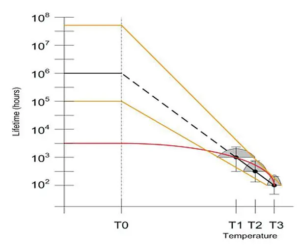
device junction temperature, among other factors. The extrapolation of the Arrhenius model along a lognormal plot across several decades of time is highly sensitive to the placement of the temperature-failure time data under the accelerated life testing (Figure 1). As shown in this paper, the inability to sample a device set and measure device temperature to a high degree of confidence can lead to a large uncertainty as to the predicted lifetime of the device.
Figure 1. Arrhenius operational life prediction (@ T0) using data extrapolated from accelerated life test data (black). Orange curves show effect of uncertainty in device junction temperature on predicted lifetime. The red curve shows a potential outcome of a set of devices where the log-linear extrapolation assumption is not valid
3. Experimental Description
Two hundred discrete GaN-on-SiC high electron mobility transistors (HEMTs) were purchased from a
commercial source and then packaged by a separate commercial entity. Twenty of those packaged devices were sampled from the population and run through a battery of three empirical tests: 1) mid-wave infrared (IR) thermography, 2) transient thermal testing (TTT), and 3) micro-Raman thermography (µRT).
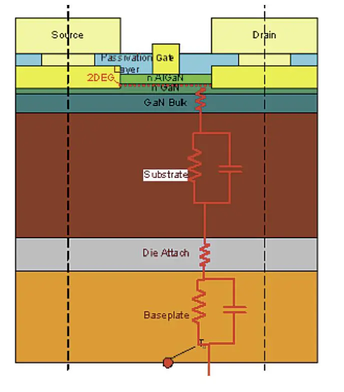
Figure 2.(Top) Schematic of the device cross section including heat flow path and (bottom) top view of device with schematic magnification of a finger with corresponding measurement technique spatial resolutions.
The average thermal resistance is given by the following equation
where Tmeas is the measured temperature, Tcoolant is the ambient coolant temperature of the heat sink, and Pdiss is the power dissipated across the device (drain current times drain voltage). It is recognized that some uncertainty in the measurement of Tcoolant and Pdissexists but that this uncertainty is negligible compared to the uncertainty in Tmeas.
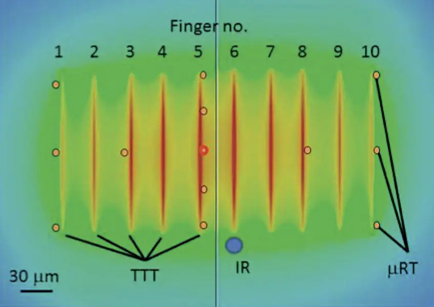
Since each of the empirical techniques measures temperature at different locations on the device surface (Figure 3), the expectation is that each method will capture different temperatures.
Figure 3. Location of empirical measurements for each technique – Infrared (IR), micro-Raman thermography (µRT), and transient thermal tester (TTT) on computationally simulated temperature contour plot of device junction plane.
The IR measurement, which was obtained using a mid wave (3-5mm) sensor, provided a minimum spatial resolution of about 10mm, larger than the distance between the gap between the gate metallization and the drain (Figure 2). Thus this measurement was made farthest from the device gate where most of the heat is generated, and so should result in the lowest temperatures. Conversely, the µRT measurement, performed with a 488nm laser, provides spatial resolution on the order of 750 nm. Thus this technique can resolve the gap between the gate and drain metallization and should come closest to capturing the peak device junction temperature. The third technique, the transient thermal tester, is a non-optical technique which measured the electrical response of a device to an electrical excitation in order to deduce the thermal resistance-capacitance network that must exist. This technique measures the average response across the entire active region of the device, and so, the TTT and spatially averaged µRT measurements should compare closely, as both sample across the gates and provide device junction temperature from both colder and warmer regions of the device.
A fully three-dimensional computational fluid dynamics model was also performed (Figure 3) using property and geometric data from the device manufacturer, packaging manufacturer and from open literature sources.
All geometric detail was included in the model around the device periphery. The heat generation site was modeled as a small volume directly under the gate metallization along the plane of the two-dimensional electron gas (2DEG) and the baseplate of the device was modeled with an isothermal boundary condition.
4. Results
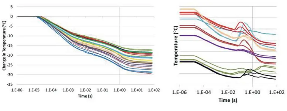
Since the devices are experiencing a step down in drain current, the device temperature should decrease steadily from a hot state to a cool state, corresponding to a steady decline in voltage. For a majority (13 of 20) of the devices, this steady decline was evidenced as seen in Figure 3. Each tested device corresponds to a color and each trace of a particular color represents one of the three tests for that device. Note that the colors are tightly spaced, which indicates good experimental repeatability. The spread of the thermal transient curves after 100 seconds is about 13°C across the 13 tested devices. This corresponds to a range in thermal resistance across the sample of 9-13 K/W.
Figure 4. Thermo-electrical response of devices to the electrical step using the TTT approach. Note that subset of tested devices on the right shows a non-thermal electrical response between 10 ms and 1s
However, a subsample of the devices exhibited a nonthermal phenomenon at a time on the order of 10 ms to 1 s after the step down, where the drain voltage increased (Figure 4, right). Since there is no source of additional heating that could cause the voltage to increase, the phenomenon must be a non-thermal electrical phenomenon. At the point of this writing, the cause of that phenomenon is not clear. One unverified suspicion is that charge trapping in the device is a potential culprit.
Micro-Raman results were studied in two ways, 1) attaining the peak point temperature measured of the 13
prescribed locations and 2) a spatially-averaged measure across the 13 measured points. The peak temperature should be indicative of the hottest temperature on the active device, which in theory, is thought to drive device failure. Based on an idealized model, the expectation is that the peak temperature should be the center-most location on the centermost gate finger. In practice, the Raman measurements do not necessarily follow that pattern. Across this sample of 19 devices (one device proved impossible to measure due to topological variability scattering the Raman signal), the peak temperature for the device occurred at 7 of the 13 prescribed points. Most of the peak temperature measurements were made along the center gate finger (12 of 19) and only 1 occurred along the perimeter finger. If the temperature at each of the 13 locations is averaged across the 19 devices, the thermal resistance measurement for each point appears in Table 1.
| Finger No: |
1 |
3 |
5 |
8 |
10 |
| Source End | 10.45 | 13.55 | 10.12 | ||
| 1/4 | 13.17 | ||||
| Center | 11.75 | 12.65 | 13.01 | 12.75 | 11.08 |
| 3/4 | 12.47 | ||||
| Drain End | 9.51 | 10.26 | 8.69 |
Table 1. Thermal resistance (K/W) for each prescribed micro-Raman measurement location and averaged across 19 devices. Finger location as indicated in Figure 2.
When averaged across the device sample set, the predicted thermal gradient perpendicular to the gate fingers is seen empirically. However, the predicted parallel gradient is not seen along the center finger. Along that finger, the hottest location does not appear to be at the finger center, but at the source end of the finger. This deviation from prediction may be due to the model simplification where metallization off the ends of the gate fingers were not included.
The Raman measurements have the highest standard deviation of the three empirical techniques, due to several factors: 1) the high precision of the technique combined with a limited sampling of spatial data points on the device surface (as compared to the TTT technique which is an analog measurement across the entire device) and 2) a high sensitivity to topological variability across the device surface. Nonetheless, the peak Raman measurement assesses a thermal resistance within 5% of the device manufacturer’s specified thermal resistance for this family of devices. Furthermore, it is worth noting how closely the average Raman measured thermal resistance (11.5 K/W) compares to the TTT approach (11.4 K/W), confirming expectations (Table 2).
| Mean Rt | St. Dev. | Tj-Tb range @ |
68% confidence (K/W)(K/W)(K)IR8.51.528 < T < 40TTT11.41.141 < T < 50µRT avg11.52.436 < T <56µRT peak15.02.948 < T < 72CFD Model15.3
Table 2. Summary of statistics for device thermal resistance as a function of measurement technique
The initial CFD model underpredicted the device vendor specified thermal resistance within 5%. Relating this information back to Figure 1, an unfortunate selection of devices could result in a significant portion of a radar system failing an order of magnitude or more sooner than expected based on the mean-time-to-failure data generally supplied by the manufacturer.
5. Conclusions
A multi-tool approach to assessing device junction temperature and thermal performance has been shown. Each tool provides different information and uncertainties so that such a broad empirical assessment is important to determine junction temperature and thermal performance. The thermal variability of packaged devices can be high. As such, an end user must view the assumption that the device junction temperature is known in the assessment of the Arrhenius reliability model with a degree of skepticism (Table 2).
To increase confidence in accounting for such uncertainty one should consider
• Instituting part-specific thermal models
• Increasing statistical sampling – use additional acquisition cost to defray future refurbishment cost
• Monitoring quality improvements in manufacturing and packaging processes
Acknowledgments
This material is based upon work supported by Naval Surface Warfare Center, Crane Division through the Naval Sea Systems Command under Contract No. N00164-09-CGR34. Any opinions, findings and conclusions, or recommendations expressed in this material are those of the author(s) and do not necessarily reflect the views of NSWC Crane or the Naval Sea Systems Command.
References
[1] Interdepartmental Committee for Meteorological Services and Supporting Research, “Federal Research and Development Needs and Priorities for Phased Array Radar (FCM-R25-2006),” Office of the Federal Coordinator for Meteorological Services and Supporting Research, Washington, DC, 2006.
[2] W. L. Pribble; J. W. Palmour; S.T. Sheppard; R.P. Smith; S.T. Allen; T.J. Smith; Z. Ring ; J.J. Sumakeris; A.W. Saxler; J.W. Milligan; “Applications of SiC MESFETs and GaN HEMTs in power amplifier design,” Microwave Symposium Digest, pp. 1819-1822, 2002.
[3] D. S. Green; B. Vembu; D. Hepper; S.R. Gibb; D. Jin; R. Vetury; J.B. Shealy; L.T. Beechem;
S. Graham;, “GaN HEMT thermal behavior and implications for reliability testing and analysis,” Physica Status Solidi, vol. 5, no. 6, pp. 2026-2029, 2008.
[4] T3ster™, Mentor Graphics
[5] ANSYS-Fluent


