Bruce Guenin
Assoc. Technical Editor, Electronics Cooling
INTRODUCTION
JEDEC single-chip package thermal metrics are widely used as a means of characterizing the thermal performance of semiconductor packages. They correlate the peak temperature of a uniformly-heated semiconductor chip (the junction temperature, TJ) with the temperature of a specified region along the heat flow path. The values of these metrics are determined from temperature measurements under standardized conditions, which specify the test method, test board, and thermal environment in rigorous detail [1].
These metrics take the form of an Ohms law resistance calculation. Thermal resistances are calculated using the equation:
where TX is the temperature of the region to which the heat is flowing and P is the total power dissipated in the device.

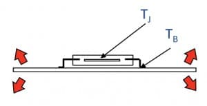
The junction-to-case and junction-to-board test environments force nearly 100% of the heat to flow along the indicated path.
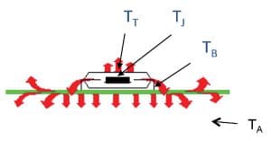
The natural convection and forced-convection environments bear a closer resemblance to most of the end-use environments for electronics than do the other two. In these convection-cooled environments, the packages lose a portion of the dissipated heat to the air out of the top surface and the remainder to the board. To a reasonable approximation, for most applications, the two paths account for nearly all of the heat flow out of the package.
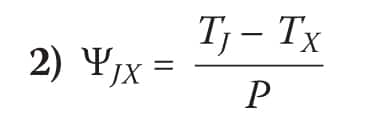
There is another class of JEDEC thermal performance metrics that are very useful in calculating junction temperatures for an application environment. They are called thermal characterization parameters and are represented by the Greek letter Ψ (pronounced “psi”) [1]. They are calculated in the same fashion as the theta metrics, as follows:
A key difference between a thermal characterization parameter and a thermal resistance is that in the case of the former, only part of heat flows to the region represented by the temperature, TX. They are useful in estimating TJ, when TX and P are known. The metrics that are most relevant to our purposes here are ΨJT and ΨJB, where TT represents the temperature at the top center of the package and TB is the board temperature, measured on a surface trace to which the package is soldered within a 1 mm distance from the edge of the package. The trace should contact the package at the middle of one of its sides.

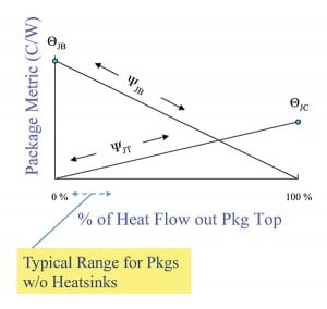
A simple model can be exploited to gain additional insight into the thermal performance of the package/board assembly. Figure 2a represents the two heat flow paths using a simple thermal resistance network. The division of the total heat between these two paths is ultimately determined by the total thermal resistance along each path, which are equal to ΘJC + ΘCA and ΘJB + ΘBA, respectively. The resistances ΘCA and ΘBA represent the efficiency of heat transport from the top of the package and the board, respectively, to the ambient air and are each a function of the air velocity. Unless a heat sink is attached to the top of the package, ΘBA will be considerably less than ΘCA due to the much larger area of the board surfaces for exchanging heat to the air compared to that of the top of the package. An inspection of this circuit shows that changes in air velocity will modify the values of ΘCA and ΘBA , leading to changes in the power flowing along the two paths and subsequent changes in ΨT and ΨB and in ΨJT and ΨJB.
The diagram in Figure 2b illustrates the interrelationship between ΨJT and ΨJB as the power flowing out the top of the package (PTOP) changes. It shows how at small values of PTOP, nearly all the power is flowing to the board and ΨJB approximates the value of ΘJB. Conversely, if a heat sink is attached to the top of the package, such that PTOP nearly equals the total power, then ΨJT approximates the value of ΘJC.
This article explores the relationship of these various metrics and how they can be used 1) with an existing electronic system to estimate the junction temperature or 2) to predict the junction temperature for a system during the design process.
Behavior of JEDEC Thermal Metrics in Forced Air Test Environment
Figure 3a contains a graph of several metrics measured on a 35 x 35 mm, 388 ball, PBGA package with a 4-layer laminate containing two copper planes. The package was mounted to a 100 mm sq. JEDEC-standard board with two copper internal planes. The two upper curves are ΘJA and ΨJB. A third curve, ΨBA was obtained by subtracting ΨJB from ΘJA.
The ΘJA curve displays a significant dependence on the air velocity, primarily due to the role of the board as a fin as it exchanges heat with the convective air flow over its entire area.
In contrast, ΨJB is nearly independent of air velocity. This results from the fact that most of the heat flow from the junction flows to the board by way of an internal conduction process. This suggests that ΨJB is relatively robust and is an effective measure of the heat conduction efficiency of the package with a relatively small contribution of the convective environment.
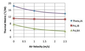
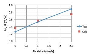
Figure 3b plots ΨJT versus air velocity. As expected, it is a sensitive function of air velocity, since the heat flow from the die through the overmolded plastic cap is proportional to the heat transfer coefficient associated with a certain air flow velocity. One notes also that at air velocities up to 2.5 m/s, ΨJT is less than 1˚C/W. The implication of this is that for modest power levels, the temperature of the top center of the package is only slightly cooler than the junction. This serves to reduce the error in calculating TJ since the value of ∆TJT calculated using Equation 2 would then be a very small correction to add to the much larger measured value of TT.
This analysis leads to the conclusion that the main value of ΨJB is that it is moderately robust and can be used to predict the temperature difference between the junction and a board, when the dissipated power is known. Conversely ΨJT is more useful if one has an operating electronic system in front of him and wants to know the die temperature in a plastic package by a measurement of the temperature at the top of the package.
It is not always the case that ΨJT is provided by the package vendor. In this situation, it is relatively easy to calculate it.
In a previous column, the following equation was derived [6]:
where h is a value of heat transfer coefficient calculated at the air velocity of interest, and tEMC and kEMC are the thickness of the epoxy mold compound above the die and its thermal conductivity. In the present example, tEMC and kEMC are 0.86 mm and 0.7 W/mK, respectively.
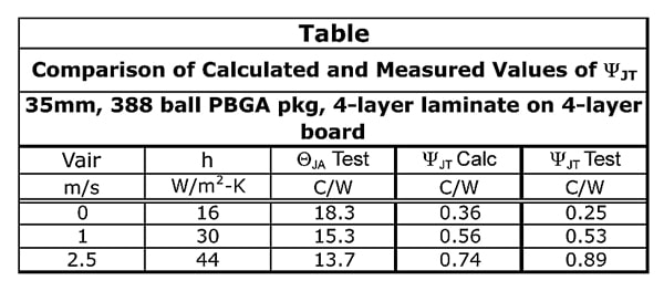
The calculated values of ΨJT are plotted in Figure 3b and are also listed in the table below along with the remaining parameters input into Equation 3. The differences between the measured and calculated values of ΨJT are small in absolute terms.
Using ΨJB is to Predict Junction Temperature in a Design
In order to successfully use the ΨJB metric in predicting the junction temperature, one needs to know TB and the dissipated power and air flow conditions in the application.
There are numerous methods available for getting an estimate of TB. Among the options is to build a load board, having the overall dimensions and conductivity of the actual board and applying the expected heat loads using heaters and also an appropriate cooling method [7]. Alternatively, one could create either an appropriate computational fluid dynamics (CFD) or finite element or finite difference conduction model of the board and accounting for the heat loads and cooling. Lastly, if a quick and moderately accurate solution is needed, it is possible to estimate the board temperature by including a single-package board in the model. The appropriate board size would be determined by taking the area of the actual board and multiplying by the ratio of the power of the device of interest to the total power due to all the devices on the board [8].
The usefulness of ΨJB, which is generated in a standard test environment, to the prediction of junction temperatures in an application results from the fact that in both environments, there is a convective boundary condition applied to the top of the package, which, ideally, would be at the same air velocity.
In general, a single resistance link from the die to the top of the package is not consistently accurate for an arbitrary boundary condition. To have robust boundary condition independence requires a compact thermal model, for example [9].
The initial work devoted to the development of the ΨJB standard showed similar values for a given package whether it was tested on JEDEC-standard multilayer boards or on an application board [10].
CONCLUSION
The JEDEC-standard thermal characterization parameters, ΨJB and ΨJT, can be valuable in facilitating the calculation of the junction temperature in a semiconductor package both for a live system and also in a predictive calculation. These metrics, determined by measurement, complement a purely thermal simulation approach by providing convenient experimental validation of simulated junction temperatures.
REFERENCES
1. JEDEC Standard JESD51-12, “Guidelines for Reporting and Using Electronic Package Thermal Information.” All JEDEC standards are available for download at no charge from www.jedec.org.
2. JEDEC Standard JESD51-2A, “Integrated Circuits Thermal Test Method Environmental Conditions – Natural Convection (Still Air).”
3. JEDEC Standard JESD51-6, “Integrated Circuit Thermal Test Method Environmental Conditions – Forced Convection (Moving Air).”
4. JEDEC Standard JESD51-14, “Transient Dual Interface Test Method for the Measurement of the Thermal Resistance Junction to Case of Semiconductor Devices with Heat Flow Trough a Single Path.”
5. JEDEC Standard JESD51-8, “Integrated Circuit Thermal Test Method Environmental Conditions — Junction-to-Board.”
6. B. Guenin, “Determining the Junction Temperature in a Plastic Semiconductor Package, Part I,” ElectronicsCooling, Vol. 5, No. 2, May, 1999.
7. B. Siegal, “Thermal Load Board Design Considerations,” ElectronicsCooling, Vol. 18, No. 3, September, 2009.
8. B. Guenin, “Characterizing a Package on a Populated Printed Circuit Board,” ElectronicsCooling, Vol. 7, No. 2, May, 2001.
9. S. Shidore, “Compact Thermal Modeling in Electronics Design” ElectronicsCooling, Vol. 13, No. 2, May, 2007.
10. B. Joiner “Use of Junction-to-Board Thermal Resistance in Predictive Engineering,” Electronics Cooling, Vol. 5, No. 1, January, 1999.

