Anurag Gupta, David H. Altman, Daniel P. Resler
Raytheon Integrated Defense Systems
Introduction
Electrical resistors are often used to simulate heat-dissipating electronic devices in thermal characterization of semiconductor devices. This article describes a study in which test measurements and analysis were conducted in steady-state conditions to characterize the thermal performance of an RF device stack-up using resistance thermometry. Discrepancy between the test-measured and numerically predicted thermal resistance results was traced back to the potential presence of an extraneous electrical resistance in the resistor circuit, or an unexpectedly poor thermal interface, with the two being indistinguishable from the data. This intertwining of electrical and thermal resistance can make accurate thermal characterization of devices and their constituent components difficult under steady-state conditions and illustrates the pitfalls of this methodology.
Experiments
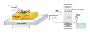
The purpose of the study was to characterize the thermal performance of the constituent components of an RF device package, as shown in Figure 1(a). The device, comprising of the resistive heater, was bonded to a metallic heat spreader with gold/tin (AuSn) solder. The spreader, in turn, was bonded to a Copper or a Copper-Molybdenum mounting bar with indium solder [1]. The mounting bar tab was bolted on to an Al baseplate. The objective of the test configuration was to characterize various spreader and thermal interface material (TIM) combinations to verify the optimal thermal packaging configuration. The resistive heater was used both as a heat source and a thermometer, the schematic of which is shown in Figure 1(b).
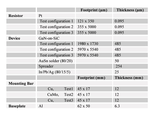
Three tests were conducted, with the details for different configurations given in Table 1. Test configuration 1 involved a 121µm x 350µm resistor, while tests 2 and 3 had larger resistors, 355µm x 5000µm each.
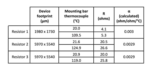
The temperature-resistance relationship of the heater was calibrated from 20oC to 120oC by adjusting the baseplate temperature while passing a small current through the resistor so not to generate appreciable self-heating. The resistance of the heater was calculated by the measured voltage drop and current for each test temperature, thereby establishing the temperature coefficient or resistance. As anticipated, the measured electrical resistance-temperature curve for these Pt resistors was essentially linear. Each R vs. T curve was represented as:
with Ro being the nominal resistance at room temperature, To, of approximately 20oC; and α, the derived constant from calibration. Table 2 shows the measured quantities used to establish the R vs. T curve. The values of α are in reasonable agreement with the reported numbers for thin Pt films [2].
With this relation established, testing was performed for the test configurations presented in Table 1. Each test involved gradually increasing the heat dissipation in the resistor in several increments such that the lowest applied heat load resulted in minimal ohmic heating, while the highest applied load maintained the resistor operating temperature at 130oC. For all tests, a temperature of 30oC was maintained at the thermocouple in the mounting bar for all power levels. The measured thermal resistance (mm2–oC/W) was calculated using equation (2), normalizing for device footprint and enabling comparison of data collected with devices of varying footprint.
Analysis

Detailed finite element (FE) models were created to represent the set-up described in the “Experiments” section with the goal of replicating the experimental data and verifying understanding of constituent thermal properties. Figure 2 shows the details of the FE modeling performed with a commercial software [3].
Material properties were applied and heat load was modeled as a uniform heat flux over the resistor area. The Al baseplate fixed-temperature boundary condition was adjusted until the thermocouple location in the mounting bar matched the test temperature of 30°C.
Results
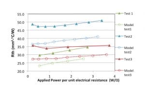
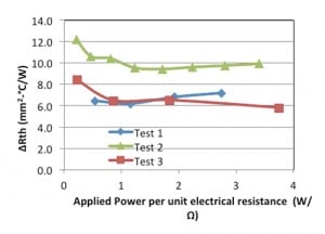
Experimentally measured and numerically predicted thermal resistance results are compared in Figure 3 for three test configurations under consideration. Applied power has been normalized by the nominal electrical resistance at 20oC to enable comparison of device testing with different power dissipations. Observed experimental and analytical trends are as expected, with thermal resistance increasing due to the decreasing thermal conductivity of SiC with increasing temperature. However, analytical predictions consistently under predicted the experimental data, requiring further investigation into potential discrepancies.
The experimental and analytical set-ups were carefully evaluated to establish repeatability. The following potential causes were investigated as a cause of the difference between the measurement and analysis.
Analysis-Induced Potential Errors
1) Modeling errors, software issues, inadequate mesh density – Analysis was conducted in two different software packages [3, 4]. Model predictions were mesh independent and results were replicated between the two software packages.

2) Application of power as uniform heat flux on the resistor area – Multi-physics electro-thermal modeling [5] confirmed a non-uniform distribution of heat flux over the resistor area due to the temperature-dependent electrical resistance of the heater. Figure 4 shows the results for Test 1 configuration at approximately 8 volts or, 11W of heat. Non-uniformity in current density is observed to be within a ±1.5% band around a mean of 1.275e+11 A/ m2, and ±6% for heat flux around a mean of approximately 3e+8 W/m2. Larger current flow resides around the edges, producing a large heat flux along the periphery.
Despite a small non-uniformity in heat flux, the temperature profile predicted at the resistor was very similar between the thermal-only and electro-thermal models. Hence, treating the heat flux as uniform in thermal simulations was deemed adequate.
3) Uncertainty in the knowledge of material properties – Indium solder was estimated to be the primary contributor, and was a source of investigation as discussed below.
Test-Induced Potential Errors
1) Heat loss from the test set-up to the environment – Any uncharacterized heat loss in equation (2) would result in the measured thermal resistance being lower rather than being higher than the model. Natural convection losses were assessed based upon a conservative heat transfer coefficient of 10W/m2K and found to be negligible. There were no parasitic conduction paths present in the experiment.
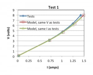
2) Unintended introduction of electrical resistance or leakage current – This was illustrated by electro-thermal modeling conducted two ways, 1) keeping the electrical voltage the same as tests and computing the electrical current, and 2) keeping the electrical current the same as tests and computing the voltage drop across the resistor. The results are shown in Figure 5 for test 1 only, but the behavior remained similar for all tests.
As evident in Figure 5, models predicted a larger current for the same applied voltage as compared to tests. One potential explanation for this result is current leakage, perhaps to another electrical resistance in parallel. This is also consistent with the prediction of a lower voltage drop for the same current, as if an unintended electrical resistance was introduced in series with the Pt resistor. The reader may note that although the V-I behavior of tests and model looks similar in Figure 5, even a small difference can be quite substantial in terms of temperature due to the very small temperature coefficient of resistance of 0.003 Ω/Ω/ oC (Table 2).
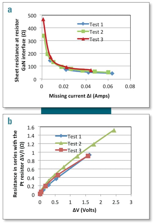
If it is assumed that the same-voltage model (same as tests) best represents reality, an extraneous electrical resistance can be synthesized as a function of the missing current. This would, for example, be an electrical resistance due to poor electrical contact between the resistor and the underlying GaN layer to which it interfaces, among other possibilities. Figure 6 shows the predicted behavior of the potential extraneous electrical resistance, which exhibits good qualitative and quantitative correlation for all tests. On the other hand, if it is assumed that the same-current model represents reality, an additional resistance in series with the Pt resistor can be modeled, again shown in Figure 6. The behavior of the extraneous resistance appears to be consistent across different tests. The resistance in each case shows a strong non-ohmic behavior in which the slope of V-I curve is not constant.
Alternatively, if a similar curve for thermal resistance is presented, as in Figure 7, a fairly constant missing thermal resistance of 6 mm2–oC/W is observed for tests 1 and 3, and about 10 mm2–oC/W for test 2. The electrical resistance in Figure 6 (a) and (b) and the thermal resistance in Figure 7 are all equivalent from the standpoint of explaining the discrepancies between the experimental data and analyses. Any of those could be the source of observed discrepancy in Figure 3.
Figures 6 and 7 illustrate that electrical resistance can appear as thermal resistance in tests and vice-versa. There is no easy way of distinguishing between the two, which leaves the experimentalist with the question as to whether thermal or electrical phenomena are responsible for the measured result, and therefore an inability to draw the desired conclusions on thermal performance.
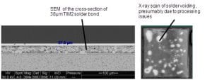
To resolve this, SEM images of the device cross-section and X-Ray inspection was performed to evaluate the quality of the indium solder bond. As Figure 8 shows, indium solder was observed to be about 1.5-2X the expected thickness, was porous and exhibited voiding over approximately 50% of the area. These results and subsequent testing strongly pointed to a degraded thermal interface to be the most likely cause; however, it was not possible to definitively rule out the possibility of electrical phenomena influencing the measured thermal performance in experiments conducted using these custom resistor-thermometer devices.
Conclusions
The use of electrical resistance is prevalent as means to simultaneously dissipate heat and measure temperatures of simulated micro-electronic devices in their packaged environment. It’s a time-tested technique that is robust and provides meaningful answers. However, just like any metrology method, it is not fool proof and there are pitfalls that an engineer must consider. This article summarizes some of the potential pitfalls, such as the intertwining of electrical and thermal resistance in certain situations, possibly leading to erroneous conclusions about thermal performance.
References
- Indium Corporation of America, Europe and Asia, www.indium.com, Indalloy#2.
- Lacy, F., “Investigating Thin Films for Use as Temperature Sensors”, Proceedings of the World Congress on Engineering and Computer Science 2007, WCECS 2007, October 24-26, 2007, San Francisco, USA.
- ANSYS Mechanical V12.0, www.ansys.com.
- ANSYS TAS V11.0.15
- ANSYS Multiphysics V12.0.
ABOUT THE AUTHOR
David H Altman is a Senior Principal Mechanical Engineer in Raytheon Integrated Defense Systems Advanced Technology Programs. David has 11 years of experience designing, developing, analyzing and testing thermal management systems for radar and other high power defense electronics systems. Over this period, David has developed liquid cooling systems, cold plates, heat exchangers and integrated thermal management systems that are employed in fielded Raytheon products. As a member of Advanced Technology Programs, his current work focuses on development of new thermal management and energy system technologies through internal (IR&D) and external (e.g., DARPA/ONR) funding. David holds BS and MS degrees from Rensselaer Polytechnic Institute and Boston University. He has authored or co-authored ten peer reviewed technical publications and holds two US patents, with seven published applications pending.


