Thomas Brunschwiler, Gerd Schlottig, Hubert Harrer and Stefano Oggioni
Abstract
In this report, the design and performance of a thermally enhanced laminate called thermal power plane (TPP) is reported. It enables dual-side electrical interconnects to a chip stack and thus supports increased communication bandwidth and power density. In addition, in a two-die stack, all through-silicon vias for power can be eliminated, with the advantage of gained silicon active area. The use of two laminates also allows individual test and burn-in of the dies prior to stack formation.
The TPP must provide efficient heat removal and current feed in the out-of-plane and the in-plane direction, respectively. An 8+1 core-less build-up laminate with aligned and stacked thermal laminate vias (TLVs) was designed and implemented. Rail-shaped solder interconnects join the TPP to the top side of the chip stack, achieving better heat dissipation capability than solder balls. In principle, the solder interface and the TPP with their thermal impedances of 4.8 and 7.4 K-mm2/W, respectively, represent an electrical functional thermal interface material1 (TIM1) and lid, with a performance that is equivalent to that of electrical non-functional TIMs and lids used in state-of-the-art packages.
Introduction
Vertical integration of integrated circuits (ICs) by through-silicon vias (TSVs) provides the prospect of high interconnectivity and close proximity of circuit elements in individual tiers. Therefore, compute performance improvements and efficiency scaling can be expected [1, 2].
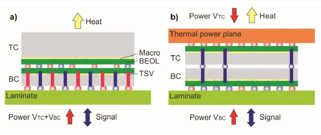
Current approaches to interface to chip stacks are equivalent to traditional packaging topologies of a single die with single-side electrical interconnects (SS-EIC) at the bottom side and heat dissipation through the top face of the chip stack (Figure 1a). However, the interface area stays constant irrespective of the number of integrated dies, and hence, may not satisfy the power delivery, signaling and heat removal requirements of high-performance chip stacks [3]. Power delivery is a challenge already in current single-die microprocessor packages, requiring up to 80% of the electrical interconnects available [4, 5]. In addition, a large number of power TSVs are needed in the bottom dies of a chip stack, resulting in significant silicon real-estate losses [6, 7].
Therefore, we proposed a novel dual-side electrical interconnect (DS-EIC) packaging concept [8]. The number of EICs to the chip stack can be doubled, and all power TSVs in a two-die stack can be eliminated by means of back-to-back bonding (Figure 1b). The enabling element is an additional laminate assembled at the top side of the chip stack (Figure 1b, orange layer). This element must be capable of providing power while imposing a low thermal resistance for the heat dissipated to the back-side cold plate. Hence, it is referred to as thermal power plane (TPP). Moreover, the integration of two laminates enables individual test & burn-in of dies prior to stack formation.
Figure 1: Cross-sectional view of a module with a two-die chip stack. a) Single-side EIC, b) dual-side EIC. Color coding: red: power, blue: signals, yellow: heat.
Single- vs. Dual-Side Electrical Interconnect Benchmark
To demonstrate the benefits of the dual-side EIC approach, a high-performance core–cache stack is considered. The high-power die (250 W, 6.8 cm2) is placed close to the cold plate to meet the temperature budget available [3]. Therefore, the 16 cores are implemented in the top chip (TC), assembled on the bottom chip (BC) with integrated L3 cache.
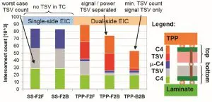
An interconnect count analysis considering typical off-chip and core-to-cache interconnect counts was performed to benchmark individual packaging topologies [8]. Five arrangements were compared, namely, single-side (SS) EIC with face-to-face (F2F) and face-to-back (F2B) and dual-side (DS) EIC with F2F, F2B, and back-to-back (B2B). The bottom laminate provides signals and power to and through the BC, whereas the top laminate (TPP) only delivers power to the TC.
The largest numbers of BC TSVs and µ-C4s are required in the single-side F2F case, closely followed by the F2B configuration, as all powering and signaling is performed through the bottom laminate (Figure 2). However, in contrast to the dual-side topologies, those configurations require no TSVs in the TC. The power to the cores in the TC is provided through the TPP in the dual-side EIC, which allows a doubling of the C4 interconnections to the chip stack. However, the dual-side F2F option still needs a large number of TSVs. For the dual-side F2B case, all power and signal TSVs can be separated to the TC and BC, respectively, which would allow an optimized TSV design depending on their functions, while maintaining only one TSV type per chip. The lowest number of TSVs results in the dual-side B2B case: The remaining TSVs only serve signaling purpose. Compared with the SS-F2F option, the silicon real-estate loss in the bottom die for the DS-B2B option can be reduced from 3.7% to 0.4% at a TSV keep-out zone of 30 × 30 mm2.
Figure 2: Interconnect count for the single-side and dual-side EIC options considered.
Design of the Thermal Power Plane
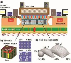
The physical implementation of the dual-side EIC concept relies on three essential packaging elements: 1) the thermal power plane (TPP), 2) elongated solder top interconnects, called rails, and 3) an on-module voltage-regulation module (VRM) (Figure 3a). The TPP needs to be a substrate with excellent lateral power delivery and vertical heat dissipation capabilities so that currents are conducted at minimal voltage drop and the heat is dissipated efficiently to the back-side liquid cold plate (Figure 3b). These two properties can only be achieved at the price of compromised electrical functionality. Hence, in the TPP, only lateral power feed with Vdd and GND domains is considered. Signaling and power feed to the bottom chip are provided by the bottom laminate (Figure 1b).
This constraint allows the implementation of a regular array of thermal laminate vias (TLVs) in the substrate without congestion of the signal wires. Copper-filled thermal vias can be achieved in coreless built-up laminates. TLVs are formed by laser drilling and subsequent electroplating. The vias are connected to individual copper planes in the laminate. The current feed capability of the laminate can be adjusted by the number of copper planes implemented, which are separated by organic dielectric layers.
Three different plane patterns are considered: bar, mesh (Figure 3b) and mesh (Figure 4). Bars run straight from one side of the laminate to the other and hence conduct the current only in a north-to-south direction. The chevron and mesh design, in contrast, support two-dimensional current feeding from any in-plane direction. The implementation of solder rails improves the thermal coupling from TC to TPP [9]. Solder Rail1 spans 3×1 solder ball locations; Rail2 spans 6×2 locations (Figure 3c).
Figure 3: a) Physical implementation of the dual-side EIC module. b) Thermal power plane topology considering bars and mesh planes. c) Top interconnect options from solder ball-to-rail arrays. (ff: fill fraction)
Implementation of the Thermal Power Plane
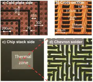
The cross-section of the coreless TPP 8+1 laminate with 18-mm-thick copper planes and 33-mm-thick dielectric layers is shown in Figure 4b. The total thickness of the laminate is 400 mm. TLVs with an average diameter of 65 mm are implemented at a pitch of 151 mm. Pairs of via rows are connected to the same domain to comply with the ground (GND) and supply voltage (Vdd) patterns of current microprocessors. This is visible in the top view of the outermost copper plane of the laminate (Figure 4a), which will later interface to the cold plate through TIM2. The underlying TLVs cause a change in the color of the copper surface and can hence be identified in pairs. In the thermal zone, solder was applied in the Rail 2 shape (Figure 3c) on the bottom side of the 50×50 mm2 TPP laminate (Figure 4c,d).
Figure 4: Photographs of a TPP with a chevron design and solder Rail2: micrographs depicting TPP a) topside and b) cross-section. c) Bottom view of the entire TPP laminate (50×50 mm2) and d) the close-up of the solder rail array, with rail length and width of 900 mm and 250 mm, respectively.
Characterization of the Thermal Power Plane
The effective thermal resistance characterization of the TPP laminates and solder interconnects was performed with a self-made bulk thermal tester [9, 10]. The TPP and solder specimens are wetted on both surfaces with liquid metal to obtain a thermal contact between two copper rods. A uniform heat flux is introduced, and the thermal gradient across the specimen and the heat flux are determined by thermocouples in the rods to derive the thermal resistance of the specimen [11].
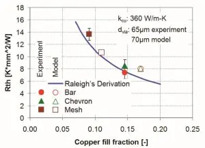
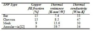
As expected from the copper via fill fraction, the effective thermal resistance of the mesh sample (5 vias per unit cell) is with 13.6 K-mm2/W substantially higher than that of the bar and chevron designs with 8 vias per unit cell resulting in close to 8 K-mm2/W (Figure 5, Table 1). Raleigh’s derivation, which was used as the analytical model and a finite-element analysis (FEA) was applied to compare the experimental results with the modeling results. Both models correctly predict the experimental values within the error margin of the experiment. Overall, the TPP thermal resistance of 7.4 to 13.6 K-mm2/W outperforms the benchmark of a thick-core laminate with annular thermal vias [12] by three to five times (Table 1).
Figure 5: TPP thermal conductivity of the bar, chevron and mesh type designs: Experimental (filled symbols) and modeling results [empty symbols: FEA; blue line: analytical equation].
Table 1: Thermal conductivity of TPP laminate. The core laminate with annular vias from [12] is listed as a benchmark case.
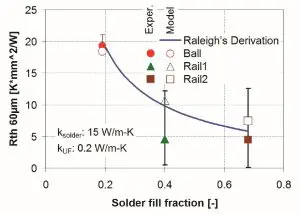
The thermal characterization of the solder interface resulted in quite a large uncertainty for the low resistances of the Rail1 and Rail2 designs. Hence, the experimental results were again supported with analytical and FEA models (Figure 6). Compared with the solder-ball array, the improvement for the Rail1 and Rail2 designs is twofold and more than threefold, respectively.
Figure 6: Experimental and modeled effective thermal resistances of the solder joints of different solder geometries at 60-µm bond-line thickness, resulting in various fill fractions (solid symbols: experiment, open symbol: FEA model; blue line: analytical equation)
Thermal Performance Benchmarking
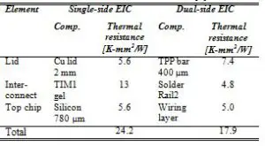
A benchmarking study of the thermal performance of the single- vs. dual-side EIC package can be performed with the available measurements (Table 2). For the single-side EIC concept, heat dissipation from top chip to cold plate occurs through the silicon die and a copper lid into the cold plate. The interfaces between the chip and lid and the lid and cold plate are filled with a TIM1 and a TIM2, respectively. In contrast, for the double-side EIC concept, heat needs to be dissipated through the wiring layers of the top chip, the solder bond-line, the TPP, and through a final TIM2 to the cold plate. The lid, TIM1, and silicon die of the single-side EIC package correspond to the TPP, the solder bond-line and the wiring layers of the top chip of the dual-side EIC package. The TPP introduces a slightly higher thermal resistance, which is compensated by the low solder thermal resistance of Rail2-type interconnects. The wiring layers of the top chip impose a similar impedance as the silicon die. In conclusion, the sum of the thermal resistances of the various elements yields a slightly lower thermal resistance in the case of the dual-side EIC approach when bar-like copper planes and Rail2-shaped solder interconnects and a gel-type TIM1 are used, as predicted in [8].
Table 2: Thermal benchmarking of single-side and dual-side EICs. Characteristic elements are described in detail in [8].
Conclusion
The benefits of the dual-side electrical interconnect topology for a core-on-cache stack were identified. They are
- twice the number of electrical interconnects to the stack, enabling larger off-stack communication bandwidth;
- elimination of all power TSVs, freeing up 3.3% silicon area, allowing optimization of the TSV design for signaling and minimization of the need for a re-design of existing macros
- individual test and burn-in of top and bottom chip, followed by stacking of known good dies, with a concomitant yield improvement.
The three main elements to implement the dual-side electrical interconnect topology were identified. They are 1)t thermal power plane, 2) solder rails and 3) on-module VRM. The thermal performance of the 8+1 coreless TPP with a thickness of 400 µm and TLVs with a mean diameter of 65 µm at a pitch of 151 µm and the solder Rail2 interconnects was identified to be as low as 7.4 and 4.8 K*mm2/W, respectively. These values are equivalent to the state-of-the-art lid and TIM1 components and thus prove the thermal feasibility of the concept.
This article demonstrates the opportunities enabled through advanced thermal packaging in system design and electrical performance of a chip package. We hope we were able to inspire thermal engineers to think in a more holistic approach in order to achieve better performance of the entire system and enable novel functionalities. Why not adding electrical functionality to a lid and to the TIM interface? That’s what the TPP and solder rails represent: they are just electrical active lids and TIMs.
Acknowledgment: The figures and tables have been reprinted, with permission, from [8] and [11]. © 2014 IEEE.
References
[1] P. Ruch, T. Brunschwiler, W. Escher, S. Paredes, and B. Michel, “Toward five-dimensional scaling: How density improves efficiency in future computers,” IBM J. Res. and Develop., vol. 55, no. 5, p. 1-13, 2011.
[2] P. Emma and E. Kursun, “Is 3D chip technology the next growth engine for performance improvement?”IBM J. Res. Develop., vol. 52, no. 6, pp. 541-552, 2008.
[3] S. M. Sri-Jayantha, G. McVicker, K. Bernstein, and J. U. Knickerbocker, “Thermomechanical modeling of 3D electronic packages”, IBM J. Res. Develop. vol. 52, no. 6, pp. 623-634, 2008.
[4] L. Minhua, S. Da-Yuan, and P. Lauro ,“Electromigration in Pb-free solders,” Proc. Int’l Conf. on Electronic Packaging Technology & High Density Packaging (ICEPT-HDP), Shanghai, China, pp. 1-8, 2008.
[5] P. Stanley-Marbell, V. Caparrós Cabezas and R. Luijten, “Pinned to the walls—Impact of packaging and application properties on the memory and power walls,” Proc. ACM/IEEE Int’l Symp. on Low Power Electronics & Design (ISLPED), Fukuoka, Japan, pp. 51-56, 2011.
[6] K. Bernstein, P. Andry, J. Cann, P. Emma, D. Greenberg, W. Haensch, M. Ignatowski, S. Koester, J. Magerlein, R. Puri, and A. Young, “Interconnects in the third dimension: design challenges for 3D ICs,” Proc. 44th Design Automation Conference (DAC), San Diego, CA, USA, pp. 562-567, 2007.
[7] N. Khan, S. Alam, and S. Hassoun, “System-level comparison of power delivery design for 2D and 3D ICs,” Proc. IEEE Int’l Conf. on 3D System Integration (3DIC), San Francisco, CA, USA, pp. 1-7, 2009.
[8] T. Brunschwiler, R. Heller, G. Schlottig, T. Tick, H. Harrer, H. Barowski, T. Niggemeier, J. Supper, and S. Oggioni, “Thermal power plane enabling dual-side electrical interconnects for high-performance chip stacks: Concept,” Proc. Electronics System-Integration Technology Conf. (ESTC), Helsinki, Finland, 2014
[9] T. Brunschwiler, Y. Madhour, T. Tick, G. Schlottig, and S. Oggioni, “Investigation of novel solder patterns for power delivery and heat removal support,” Proc. 2013 IEEE 63rd Electronic Components and Technology Conference (ECTC), Las Vegas, NV, pp. 417-424, 2013.
[10] K. Matsumoto and Y. Taira, “Thermal resistance measurements of interconnections for the investigation of the thermal resistance of a three-dimensional (3D) chip stack,” Proc. 25th Annual IEEE Semiconductor Thermal Measurement and Management Symposium (SEMI-THERM 2009), San Jose, CA, USA, pp. 321-328, 2009.
[11] T. Brunschwiler, T. Tick, M. Castriotta, G. Schlottig, D. Gschwend, K. Sato, T. Nakajima, S. Li, and S. Oggioni, “Thermal power plane enabling dual-side electrical interconnects for high-performance chip stacks: Implementation,” Proc. Electronics System-Integration Technology Conf. (ESTC), Helsinki, Finland, 2014
[12] R. Schacht, B. Wunderle, E. Meli, D. May, O. Wittler, B. Michel and H. Reichl, “Effective thermal material models for multi layer PCBs with thermal vias,” 1st Micro- NanoReliability 2007, Berlin, Germany, 2007.

