Banafsheh Barabadi, Satish Kumar, Valeriy Sukharev, & Yogendra K. Joshi
Banafsheh Barabadi
Department of Mechanical Engineering
Massachusetts Institute of Technology
77 Massachusetts Ave. Cambridge MA 02139
Yogendra K. Joshi
Satish Kumar
G.W. Woodruff School of Mechanical Engineering
Georgia Institute of Technology
801 Ferst Dr, Atlanta GA 30332
Valeriy Sukharev
Design-To-Silicon Division, Mentor Graphics Corporation,
46871 Bayside Parkway, Fremont, CA 94538
Corresponding Author:
Yogendra K. Joshi
INTRODUCTION
As the Integrated Circuit (IC) chip and package continue to scale down, the power density and thermal and electrical resistance of these devices continue to increase, resulting in the creation of local hot-spots that are dependent on layout and workload. This can cause major variation in the performance and efficiency of devices. Heat is mainly generated in the transistors which have a characteristic length scale of tens of nm (~10-8 m). The generated heat is conducted through the chip and package components such as substrate, mold compound, and heatsink and is ultimately removed from the package via convention. At the package level, the characteristic length scale is on the order of tens of cm (10-1 m). Additionally, the transient thermal events in IC devices vary from microsecond (10-6 s) at the transistor level to tens of seconds (102 s) at the package level. Therefore, Joule heating in IC devices is a multi-scale problem both in length and time scales.
To model such geometries, traditional full field finite element (FE) and finite difference (FD) methods are computationally inefficient as they require large number of computational nodes or elements. Hence, they are impractical for any parametric study. Several multi-scale modeling methodologies have been developed to determine the thermal profile in IC devices, such as thermal impedance networks [1, 2] and compact models [3]. However, they generally suffer from low accuracy in the presence of complex geometries and boundary conditions, as well as nonlinearity in the heat diffusion equation [4, 5]. Another limitation of such models is the difficulty in handling fluid/solid interactions. In addition, the majority of the previous methods have been focused on steady-state Joule heating in IC devices. In many applications it is necessary to study the effect of transient heat conduction due to the pulsed nature of the electric currents in the transistors and interconnects. Therefore, there is a need for the development of high fidelity transient multi-scale thermal models that overcomes the challenges faced by existing thermal models.
Barabadi et al. [6] developed a computationally efficient hybrid multi-scale approach for transient thermal modeling of microelectronics. The model combines two different and well-established multi-scale concepts: “Progressive Zoom-in” (e.g. [7]), and “Proper Orthogonal Decomposition (POD)” ([8]). The method is capable of modeling several decades of length scales, from tens of millimetres at “package” level to tens of micrometres at “chip component” level and to potentially several nanometres at “interconnects” (not included here) level. This characteristic of the proposed model also applies for time scales ranging from tens of seconds to microseconds corresponding to different thermal events. The hybrid scheme can also accurately and rapidly predict the thermal responses of an IC device for different power input profiles based on only a few representative detailed simulation. It is shown that the proposed model can reduce the computational time by approximately two orders of magnitude at every step of modelling with less than 8% error in simulation[9].
In this article, we briefly describe the hybrid scheme used for transient thermal modelling of a Flip Chip Ball Grid Array (FCBGA) package with an embedded die and its function blocks. To further demonstrate the capability of POD method in predicting different thermal events, randomly generated transient power distributions are assumed for the chip and its individual function blocks. The results are validated against a full-filed FE model developed in a commercially available finite element analysis (FEA) software tool [10]. For more details on this study please refer to recent publications by the authors [11, 12].
Methodology
The developed hybrid scheme integrates the implementation of POD and progressive zoom-in approach:
POD Method: POD is a robust and computationally efficient method that captures the complexity of a high-dimensional physical system and provides low-dimensional yet accurate description of it by using a reduced number of degrees of freedom [13]. POD technique expands a set of data on empirically determined basis functions, also known as modes, for modal decomposition such that the least square error between the true solution and the truncated representation of the POD model in minimized. This technique numerically predicts the temperature distribution within a system more computationally efficiently than any full-field FE or FV (finite volume) simulations. A comprehensive study on various applications of POD is provided by Holmes et al. [14]. In summary, there are four main steps in developing any POD model: The first step is to generate the observation data set which can be obtained either experimentally or numerically (this study). The second step is to calculate the basis functions a.k.a POD modes. Modes are only functions of space. The third step is to calculate the POD coefficients (functions of time). The fourth and final step is to construct the temperature field based on the POD modes and coefficients from the expansion:
where T0 is the time average of temperature (i.e., the mean vector of the observation matrix), φi(x, y, z) is the i-th POD mode, and bi(t) is the i-th POD coefficient. Thorough derivation of a 2-D POD based reduced order diffusion model is provided in [9]. The 3-D formulation of POD method for conduction heat transfer is given in [11].
Progressive Zoom-in Approach:
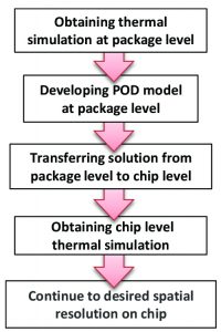
Progressive zoom-in is another multi-scale modelling technique that has been previously developed and can be used for transient thermal analysis in IC devices [15, 16]. Following a similar procedure described in [7],various levels of thermal behaviour in a system from package to chip, sub-chip, and ultimately transistor level can be integrated. This is done by passing down the acquired thermal knowledge of the system from each level to the following one through effective boundary conditions. By combining POD with progressive zoom-in approach, the computational efficiency of the hybrid model in covering several orders of magnitude in length and time scale is further improved. The overall hybrid approach for this work is shown in the flowchart of Figure 1 and is outlined below:
First, the entire package including chip, substrate, mold compound, and solder bumps is numerically modelled based on total chip power, boundary conditions, and initial conditions. At this level of simulation, chip is modelled as a solid block with effective material and thermal properties. No knowledge of chip internal features is required at this stage. Once the transient temperature distribution at package level is determined, POD model of the package is developed based on the chip power profile as previously explained. The POD model is able to predict dynamic temperature distribution for different power maps and types of power sources, without developing any further full-field finite element models [9]. This can considerably decrease computational cost and potentially be used to prescribe a criterion for the optimal distribution of the current density in the device. In the next step, a combination of heat flux and temperature on the surrounding walls of chip is extracted and applied in the form of dynamically changing boundary conditions for the chip level simulation. At this level, the chip is no longer treated as a solid block and is divided into subdomains called function blocks. Each block represents a component with unique functionality on the chip and consists of three sub-layers: 1. Silicon layer, 2. Transistor layer, and 3. Interconnect/Dielectric multilayer. The transient thermal solution at the chip level is then determined by assigning the block specific power profiles, thermal and material properties. Based on the desired spatial resolution, this approach can be continued to sub-chip level domains. In this article, the results of two levels (package and chip) is provided.
Figure 1. Flowchart of the hybrid scheme used for multi-scale transient thermal modeling.
Results and discussion
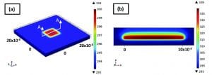
As described in the Methodology section, the first step is to determine the transient thermal profile for the entire package without chip internal details. A simplified schematic of the FCBGA package used in this work is shown in Figure 2 (a). References [17] and [18] are used as a guideline for dimensions and material selection for the package. The effective material and thermal properties of each component of the package is calculated and in-plane and through-plane thermal conductivity values of the underfill/solder bumps are also determined [11]. This package is used for low power portable systems where compact form factor prohibits the use of heat sinks and forced cooling. Therefore, natural convection boundary condition with a heat transfer coefficient of h = 15 W/m2K (typical range for air [7]) was applied to the top surface and a constant temperature boundary condition is assumed at the bottom surface. Total transient chip power is assumed to have the form Q=3sin2πt+3 (W) and is applied for 0.5 s which represent a modulating power input to the system. This power profile is chosen only to develop the hybrid scheme. Once the model is complete, temperature distribution corresponding to more realistic power profiles can be determined at a much lower computational cost. A full-field FE model of the package is then developed in consisting of 75,919 elements, of which 343 are for the chip. The convergence of the FE model is verified with respect to the solver type, time step, and time integration method and the proper grid size is determined through mesh independence analysis. The FE temperature profile in the package after 0.5 s is shown in Figure 3 (a). Figure 3 (b) demonstrates the 2D spatial distribution of temperature inside the package along the A-A cross section.
Figure 2. Simplified schematic of (a) FCBGA package used in this study for package level modeling and (b) the enclosed die with function blocks for chip level modeling.
Once the transient temperature profile is determined, a POD model is developed at the package level using the procedure described in the previous section. Twenty six observations of the transient thermal solution are taken from the package level FE model. These observations correspond to the temperature solutions obtained at different time instants during the 0.5 s simulation time. As shown by Barabadi et al. [9], for any linear system, POD method can predict transient thermal solution regardless of the temporal or spatial dependence of the applied heat source. This feature can be used to predict temperature distributions for arbitrary heat inputs, by using a smaller sample set of applied heat sources and power maps and will result in significantly lower computational time. To further verify this feature, a POD model is developed based on the original power source (Q=3sin2πt+3 (W)) for 0.5 s and applied to predict the temperature profile for a randomly varying transient power distribution between 0-18 W for 1 s. The new power profile differs from the previous power input in duration, magnitude, and temporal dependency. POD basis functions (POD modes) are calculated based on the observation data set. To have a fast but reliable reduced order model, only four modes are kept in this study. This is chosen such that the cumulative correlation energy, Em [19] of the system is greater than 99.9%. The corresponding POD coefficients are then calculated as functions of time using the method of Galerkin Projection [9]. Finally, the reduced order transient temperature profile can be determined using Eq. (1).
Figure 3. FE temperature profile after 0.5 s for (a) FCBGA package and (b) the A-A cross section (dimensions in m, temperature in K).
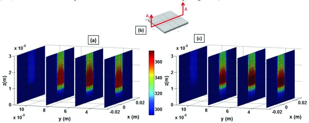
Figure 4 (a) exhibits the three dimensional temperature profile of the package using the POD model 1 s after the power profile is applied. The domain is sliced in XZ plane along the A-A cross section shown in Figure 4 (b). The right-most slice goes through the center of the chip. To validate the model, a full-field FE model is developed in in the FE software with the same grid size, element, and simulation time step used in POD model (results shown in Figure 4 (c)). The POD model closely predicts the transient thermal behavior of the system even for projected time outside of the original time domain when t >0.5 s. The mean absolute error between the POD and FE model is 7.2 % over the entire space and time domain. The computation time required for FE simulation is approximately 30 to 100 times higher than that of POD (23.7 min vs. 40 s respectively). The first POD simulation run-time is 40 s. Any additional POD simulations with different power profiles take 15 s each.
Once the transient thermal solution is obtained at the package level for 1 s, the next step in the hybrid scheme is to transfer the solution to the chip with the higher spatial resolution in the form of boundary conditions. A combination of temperature and heat flux is dynamically transferred down every 0.1 s as boundary conditions on top and bottom surfaces of the chip. Due to high aspect ratio of the chip, side walls are assumed to be adiabatic. The thermal solution is then linearly interpolated on each surface of the chip with much higher spatial resolution (268,033 elements in the chip at this level versus 343 elements at the package level).
Figure 4. Temperature profile inside the package at 1 s extracted from the POD model (a) and FE simulation (c). The domain is sliced vertically along XZ plane. The right-most slice is the A-A cross section (b) (adapted from [11]).
For chip level modelling, the die is no longer assumed to be a solid block. It is now divided into 10 subdomains called function blocks (figure 2 (b)), which represent various components on the chip with different functionalities. Each block consists of three sublayers: top silicon layer (0.249 mm thick), transistor layer (5 µm thick), and the interconnect/dielectric multilayer. The effective properties of the functional blocks are calculated based on a combination of directional volume and surface -averaging methods. The in-plane and through-plane thermal conductivity of each function block is determined by constructing the corresponding equivalent thermal resistance network. At this stage, the spatial resolution of the model is limited to the sub-layers of the blocks [11]. A dynamic power grid also needs to be assigned to each individual function block to its transistor sub-layer where the majority of the heat is generated. Therefore, ten random transient power profiles are generated separately and assigned to each block such that their sum equals the total chip power used for package level modeling.
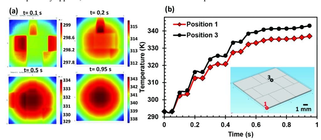
Once the power profiles are allocated to each function block, an FE transient thermal model can be developed using the calculated thermal and material properties as the final step of the hybrid approach. The FE model consists of 268,033 elements and the computational time to run the transient simulation for 1 s is approximately 26 min. Figure 5 (a) shows 2D contours of temperature profile at various times (0, 0.1, 0.5, and 0.95 s) on top of the transistor layer where maximum temperature occurs. Figure 5 (b) displays the temporal distribution of temperature at two different locations on the chip (position shown on the inset plot). In general, the procedure described in this article can be repeatedly applied, until the desired resolution on the chip is achieved.
Figure 5 (a) Spatial distribution of temperature profile at chip level on top of the transistor layer after 0, 0.1, 0.5, and 0.95 s, (b) temporal distribution of temperature at two locations on the chip.
Summary and Conclusion
An efficient and accurate multi-scale transient thermal model, using a hybrid scheme, was developed with the ability of modeling several decades of length and time scale, at orders of magnitude lower computational cost while maintaining satisfactory accuracy. Utilizing the proposed model, the computational time is reduced by 30-100 times at every step of zooming into the geometry. The proposed approach is not limited to the package, chip, and function block levels and can be scaled down to “transistor level” while taking advantage of POD method to avoid any further full field simulations. One potential application of this method is during the design stage in IC industry. The multi-scale transient model can be developed for a specific chip structure that uses output signals of temperature sensors embedded on the chip and package as the original observations. This model can be incorporated into a closed loop on-chip control system to predict and potentially avoid the possible locations of hot-spots.
Acknowledgments
The research is partially funded by Semiconductor Research Corporation (SRC) under Task 1883.001 and Design-to-Silicon division of Mentor Graphics Corporation.
References
[1] Christiaens, F., Vandevelde, B., Beyne, E., Mertens, R., and Berghmans, J., 1998, “A Generic Methodology for Deriving Compact Dynamic Thermal Models, Applied to the Psga Package,” IEEE Transactions on Components, Packaging, and Manufacturing Technology, Part A, 21(4), pp. 565-576.
[2] Lasance, C., Vinke, H., Rosten, H., and Weiner, K. L., 1995, “A Novel Approach for the Thermal Characterization of Electronic Parts,” Semiconductor Thermal Measurement and Management Symposium, Eleventh Annual IEEE SEMI-THERM XI., pp. 1-9.
[3] Krueger, W., and Bar-Cohen, A., 1992, “Thermal Characterization of a Plcc-Expanded Rjc Methodology,” IEEE Trans. Compon., Hybrids, Manuf. Technol., 15(5), pp. 691–698.
[4] Gerstenmaier, Y., and Wachutka, G., 2002, “Rigorous Model and Network for Transient Thermal Problems,” Microelectronics journal, 33(9), pp. 719-725.
[5] Celo, D., Xiao Ming, G., Gunupudi, P. K., Khazaka, R., Walkey, D. J., Smy, T., and Nakhla, M. S., 2005, “Hierarchical Thermal Analysis of Large Ic Modules,” IEEE Transactions on Components and Packaging Technologies, 28(2), pp. 207-217.
[6] Barabadi, B., Kumar, S., Sukharev, V., and Joshi, Y. K., 2012, “Multi-Scale Transient Thermal Analysis of Microelectronics,” ASME 2012 International Mechanical Engineering Congress & Exposition (IMECE2012), Paper No. IMECE2012-89864.
[7] Tang, L., and Joshi, Y. K., 2005, “A Multi-Grid Based Multi-Scale Thermal Analysis Approach for Combined Mixed Convection, Conduction, and Radiation Due to Discrete Heating,” Journal of Heat Transfer, 127(1), pp. 18-26.
[8] Lumley, J. L., 1967, “The Structure of Inhomogeneous Turbulent Flows,” Atmospheric Turbulence and Radio Wave Propagation, pp. 166-178.
[9] Barabadi, B., Joshi, Y., and Kumar, S., 2011, “Prediction of Transient Thermal Behavior of Planar Interconnect Architecture Using Proper Orthogonal Decomposition Method,” ASME InterPACK, pp. 213-224.
[10] COMSOL, 2011, “COMSOLVersion 4.2,” Comsol Multiphysics, Inc., Burlington, MA, http://www.comsol.com, last retrived August 24, 2015.
[11] Barabadi, B., Kumar, S., Sukharev, V., and Joshi, Y. K., 2015, “Multiscale Transient Thermal Analysis of Microelectronics,” Journal of Electronic Packaging, 137(3), pp. 031002-1 – 031002-8.
[12] Joshi, Y., Barabadi, B., Ghosh, R., Wan, Z., Xiao, H., Yalamanchili, S., and Kumar, S., “Thermal Simulations in Support of Multi-Scale Co-Design of Energy Efficient Information Technology Systems,” THODS FOR, pp. 75-90.
[13] Chatterjee, A., 2000, “An Introduction to the Proper Orthogonal Decomposition,” Current Science, 78(7), pp. 808-817.
[14] Holmes, P., Lumley, J. L., and Berkooz, G., 1998, Turbulence, Coherent Structures, Dynamical Systems and Symmetry, Cambridge University Press, Cambridge, UK.
[15] Tang, L., 1998, “A Multi-Scale Conjugate Thermal Analysis Methodology for Convectively Cooled Electronic Enclosures,” Ph.D. thesis, research directed by Dept. of Mechanical Engineering.University of Maryland, College Park, Md.
[16] Wilson, J. S., and Raad, P. E., 2004, “A Transient Self-Adaptive Technique for Modeling Thermal Problems with Large Variations in Physical Scales,” International Journal of Heat and Mass Transfer, 47(17), pp. 3707-3720.
[17] Incropera, F. P., Bergman, T. L., Lavine, A. S., and Dewitt, D. P., 2011, Fundamentals of Heat and Mass Transfer, Wiley, Hoboken, NJ.
[18] Chang, K. C., Li, Y., Lin, C. Y., and Lii, M. J., 2004, “Design Guidance for the Mechanical Reliability of Low-K Flip Chip Bga Package 1,” International Microelectronics and Packaging Society (IMAPS) Topical Workshop and Exhibition on Flip Chip Technology pp. 21-24.
[19] Bizon, K., Continillo, G., Russo, L., and Smula, J., 2008, “On Pod Reduced Models of Tubular Reactor with Periodic Regimes,” Computers & Chemical Engineering, 32(6), pp. 1305-1315.


