Simply stated, the problem with the use of volume weighted, effective thermal conductivity, kvw, in the thermal modeling of a printed circuit board (PCB), is inaccuracy. In this paper, we show how using kvw can lead to serious errors in the prediction of PCB temperatures. We recommend two, related, alternative procedures that provide greater accuracy.
Introduction
A common feature of the thermal analysis of electronic equipment is the complexity of the heat flow paths in the hardware. Nowhere is this more evident than the printed circuit board, where the multiple layers of complex trace patterns present a daunting thermal modeling task.
Consider a 6 layer, 100 x 100 mm (4 x 4 in), circuit board, with some traces as small as 0.25 mm (0.010 in) in width. A thermal model, either finite difference (FDM) or finite element (FEM), would require a mesh of 400 (100/.25) nodes or elements on a side or nearly 160,000 nodes per layer, resulting in almost 1,000,000 nodes for the board; and this is a relatively small PCB. A large board, say 250 x 250 mm (10 x 10 in), with 10 layers would generate a model with more than 10,000,000 nodes. Clearly, computing temperatures for a PCB model that resolves the details of the trace patterns stretches the capabilities of some PC’s.
Since the traces are important heat transfer paths, which cannot be ignored in the thermal design, analysts have resorted to a procedure in which volume weighting of the trace and board thermal conductivities is used to define a volume weighted, effective thermal conductivity, kvw. This procedure is referred to as “smearing” and kvw is defined by,

where Vt is the total trace volume, Vb is the volume of the board material, V = Vt + Vb is the PCB total volume and kt and kb are the trace and board thermal conductivities.
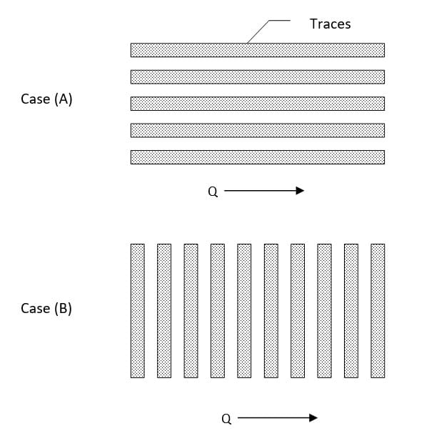
While appealing in its simplicity and intuitive reasonableness, it is not difficult to demonstrate the inherent inaccuracy of this approach. Consider two idealized trace geometries: Case (A), with all traces running parallel to the direction of the heat flow Q (parallel to the temperature gradient), and Case (B), with traces running perpendicular to the heat flow; see Fig. 1.

It is easy to see that there is no loss of accuracy with the definition of kvw for Case (A). However, using kvw in Case (B), results in significant error. We illustrate this with assumed values for the trace and board percentages and thermal conductivities.
Let the trace volume percentage be 10% and the board volume percentage be 90%. Assume the trace conductivity, kt, is 391 W/m-C and the board conductivity, kb, is 0.59 W/m-C. Then kvw = (0.10)(391) + (0.90)(0.59) = 40 W/m-C.
For Case A, this value of kvw is appropriate, and if all traces run in the same direction as the heat flux vector, there is no error.
For Case B, we can readily calculate the correct effective conductivity. Again, assuming the conduction path is 10 % copper and 90% board, the thermal resistance R, C/W, for the strips of trace and board in series is
where L is the total path length and A is the area normal to the heat flow.
The conductance G, W/C, is
This implies an effective thermal conductivity of 0.65 W/m-C. as compared to 40 W/m-C for kvw. This is a major discrepancy, and it arises whenever the traces run primarily perpendicular to the heat flow.
Modeling errors can also occur wherever there are regions of a PCB that are predominantly board material. The use of an effective conductivity such as the above value of 40 W/m-C, instead of a typical board conductivity of 0.59 W/m-C, in the calculation of heat flow across these regions is unrealistic. This will be demonstrated for a post mounted PCB by comparing board temperatures computed using kvw with those computed using a more accurate procedure described in the following section.
A New Procedure For Computing Thermal Conductances And Effective Thermal Conductivity
As pointed out in the INTRODUCTION, a finite element (FEM) model of a PCB can entail a mesh of many millions of elements, making this approach largely impractical. On the other hand, a finite difference (FDM) control volume mesh offers significant advantages. This is because each FDM control volume can encompass more board real estate than a FEM element. However, the benefits of FDM only accrue, if meaningful conductance values can be derived for the heat flow between neighboring nodes.
In the following discussion a method of calculating these conductances is presented. In addition, a procedure for obtaining a more accurate effective thermal conductivity is outlined.
The New Method
A procedure for computing PCB conductances has been presented in a paper by the author, Ref. 1. It embodies the generation of computer bitmap files for the layers of the PCB, and the subsequent use of these files as representations of the geometry of each layer. The bitmaps are obtained from CAD master patterns or other electronic design files generated during the design process
A typical bitmap file consists of a sequence of zero’s and one’s, denoting, respectively, board or trace regions. The bitmap density is selected based upon the required geometrical resolution for the thermal analysis, typically 200 pixels per inch.
Fig. 2 is a portion of a bitmap of a layer of a sample PCB. Each bitmap pixel is depicted as a small rectangular region of trace or board material. The key feature of this new approach is the computation of grid thermal conductances utilizing the geometrical information in the bitmaps.

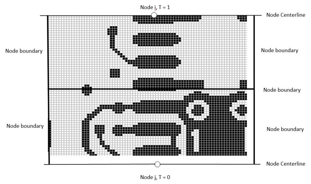
Attention is focused on the computation of a typical conductance between two nodes i and j as illustrated on Fig. 3.

What is desired is the thermal conductance Gij between node i and node j. As stated earlier this is the ratio of the heat flow between the two nodes divided by the temperature difference,
If the effective thermal conductivity keff were known, Gij could be computed from the expression,

Due to the complex patterns of circuit and board material comprising node i and node j, the effective thermal conductivity keff is not known and is difficult to estimate visually.
The new procedure for the creation of the geometric model begins, instead, with Eqn. 2 which defines the thermal conductance, Gij. The heat flow Qij is computed for a specified nodal temperature difference, and the ratio of the computed heat flow to the specified nodal temperature difference is the desired thermal conductance.
Referring to Fig. 3, the temperature of node i is specified to be unity along the centerline of node i and the temperature of node j is specified to be zero along the centerline of node j. The numerical value of the two node temperatures is arbitrary, since what is to be computed is the heat flow per unit of temperature difference.

Considering each small bitmap rectangle to be a micro-node, as distinguished from the macro-nodes i and j, allows for the generation of micro-conductances between micro-nodes. The micro- conductances are easily computed since each micro-node is either all trace material or all board material. Using this set of micro-conductances for the region between the centerlines of node i and node j, the temperature distribution and the heat flow Qij across the boundary between node i and j is computed.
From the specified temperatures of nodes i and j and the interface heat flow, the desired macro-conductance is obtained from Eqn. 3. Following this procedure for all pairs of macro-nodes in the layer under consideration gives the complete set of required conductances for the layer. This is carried out for each layer of the PCB, and employing these conductances in an FDM model produces reasonably accurate node temperatures.
A Post Mounted Circuit Board
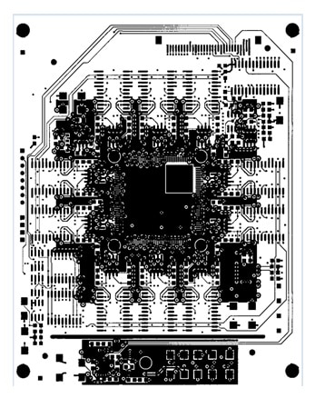
The error in employing kvw will depend upon the thermal boundary conditions to which the PCB is exposed; that is, the type of mounting hardware and the exchange of heat with its environment by convection and radiation. A common mounting condition consists of round posts at corners and possibly at interior locations. A layer of a board which is mounted on corner posts is shown on Fig. 4.

This is the top layer of a 6 layer, 100 x 125 mm (4 x 5in) board, mounted on 4 posts. Note that in order to provide isolation from electrical ground, the traces do not extend all the way to the posts. This has a major impact on the conduction of heat to the posts and subsequent heat flow to the device case and its environment.
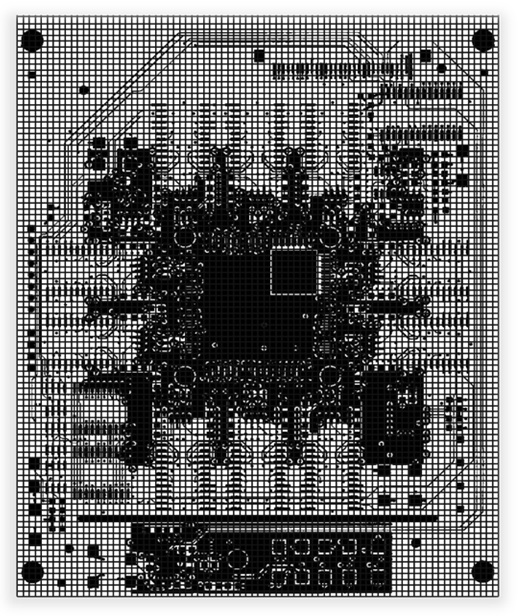
A thermal model of this board with an 80 x 100 node grid is shown on Fig. 5. This is a much finer grid than is normally required in the thermal analysis of PCB’s, but we want to minimize the discretization error when comparing results computed with and without the use of kvw.
We assume a specified temperature, 0 C, for the board at those nodes that are in contact with the posts. Then the computed temperatures represent temperature differences between board nodes at the posts and nodes at the locations of the components. We are interested in the maximum temperature difference.
The presence or absence of convection and radiation will impact the predicted temperatures, and we will obtain results with and without convection and radiation.

The board has six trace layers and a power dissipation of 1 w. The volume weighted, effective conductivity is 38 W/m-C. The computed, maximum temperatures are summarized on the following table.
It can be seen that, the use of mounting posts with no convection or radiation provides thermal paths with very high thermal impedance and the maximum board temperature is 236 C. When the thermal conductivity of the board is assumed to be the volume weighted, effective conductivity, 38 W/m-C, the calculated thermal impedance is markedly less and the maximum temperature rise is predicted to be only 9 C, an error of 227 C.
When we include convection and radiation in the heat rejection process, the correct maximum temperature is 19 C. The use of the volume weighted, thermal conductivity, kvw , predicts a temperature of 7 C, a 12 C error.
Utilizing The New Method In A FEM Model
Over the last several decades, electronic equipment thermal analysts have come to appreciate the ease with which irregular geometries can be modeled using FEM pre and post processing. However, they use volume weighted, effective thermal conductivity, in their models. To avoid this source of error and take advantage of the strong points of both FDM and FEM, the following approach is proposed:
- Compute PCB temperatures, T, employing the bitmap approach in an FDM model.
These temperatures will be assumed to be the most accurate values obtainable, short of creating a multi-million node model that properly accounts for the complex geometry.
- Compute PCB temperatures, Teff, using a trial thermal conductivity, keff. and compare Teff with T.
- Repeat Step 2 until the difference between Teff and T is minimal. This could be minimizing Teff – T at the location where the board temperature, T, is greatest, or it could be minimizing the root mean square of Teff – T.
- Using an FEM modeler and the optimum keff obtained in Step 3, compute temperatures and perform desired parametric studies, e.g., component placement, component power dissipation and boundary conditions.
This approach has been investigated for the post mounted PCB treated above, and the value of keff that yields the correct maximum temperature of 236 C, is found to be 1.5 W/m-C, not 38 W/m-C. This remarkable result is not difficult to grasp when one considers the extended region of only board material around each mounting post in a situation wherein all the heat must flow to the posts for removal.
When convection and radiation are included, the value of keff that yields the correct maximum temperature of 19 C, is found to be 11 W/m-C as compared to 38 W/m-C for the volume weighted effective conductivity, kvw.
Note that kvw , by definition, Eqn. 1, is not a function of the board boundary conditions, an obvious weakness in the utility of this parameter. We have seen that, effective conductivity depends strongly on the geometry of the heat flow paths to the environment.
These results illustrate that the use of volume weighted, effective thermal conductivity, kvw, produces unacceptably large errors in the calculation of PCB temperatures.
Conclusions And Recommendations
Using the volume weighted, effective thermal conductivity kvw in a PCB thermal model can lead to serious errors.
A new procedure is presented that utilizes the geometrical information inherent in the board layer bitmaps to compute reasonably accurate values of thermal conductances and board temperatures using an FDM model.
A related procedure is proposed that allows the analyst to employ an FDM model to compute an effective thermal conductivity, keff, that is more accurate than the volume weighted, effective conductivity, kvw. This effective conductivity can then be used in an FEM model to compute board temperatures and perform parametric studies. This approach takes advantage of the strong points of both FDM and FEM.
References
- Sampson, R. L., “Printed Circuit Board Thermal Modeling Without the Use of Effective Thermal Conductivity”, ASME IPACK2005-73013, 2005


