Co-authored by: Nitesh Kumar Sardana, Susyamala Pavan Kumar Busam, Dr. Laxmidhar Biswal
Robert Bosch Engineering and Business Solution Pvt. Ltd.
Abstract
The market demand for lightweight and cost effective electronic products with multi-functional operations leads to the introduction of plastic housing and high current density on board. In general, automotive electronic products operate in harsh environment. With high current demand, Joule heating in copper traces on the board is highly pronounced. Managing heat dissipation from components and traces without the use of cooling banks on the plastic housing is a thermal challenge.
For this study, the product consists of a plastic enclosure that houses printed circuit board (PCB) and electronic components that are capable of operation at higher current. The product consists of multiple inputs and outputs to support a variety of loads. The high current is distributed across multiple copper layers in PCB. These copper layers (due to constraints on their dimensions) experience high current densities leading to higher Joule heating. In addition, there are several heat dissipating components on board. As a result, the components are exposed to higher operating temperature. Electrical-Thermal simulation helps to (i) visualize the thermal field, (ii) identify bottlenecks to current flow, and (iii) identify hot spots in order to optimize the circuit layout for reducing the Joule heating.
In this study, Electrical-Thermal simulation is carried out using Thermal Risk Management tool (TRM). The model consists of lumped components with their respective power dissipation, thermal vias in PCB underneath the heat dissipating components, PCB base material (FR4), copper layers with discrete traces for current flow and heat conduction, and electrical nets for current flow among copper layers, input-output pins and components. The effect of enclosure is manifested in the overall heat transfer coefficient that is applied on PCB and components as boundary condition. Overall heat transfer coefficient is derived from a system-level conjugate heat transfer model accounting for conduction, convection and radiation for the entire product. Electrical current (I) is assigned to input and out pins. Ambient temperature is applied to PCB and components as boundary condition.
Measurement at board-level is carried out in the lab via Thermal imaging and thermocouple measurements for thermal field and component temperatures respectively. Simulation and measurement results are found to be within ± 3%.
After validating the simulation model, parametric study via simulation is carried out to optimize the copper traces geometry and location of components and power dissipation of the components, PCB stack up and PCB base material properties. These parameters are evaluated against the cost of the product due to each change. This optimization helps in reducing the hot spots and temperature on the PCB, during the early development phase itself, and reduces the development cost as well as the product cost.
Introduction
With the rise in usage of electronics in automobile industry, the demand for light weight and cost effective electronics has increased exponentially in the past few decades. Along with the packaging requirements, the functionality of electronics has increased, posing challenges for thermal management of electronics. To cater to numerous functions required by the application, component density and current in the Printed Circuit Board has increased too.
These requirements have led to the introduction of plastic housing and high current density on board.
The amount of heat generated in copper traces on board due to flow of current is
Q= I2R (1)
Where,
Q: Joule heating, W
I: current flow in copper traces on board, A
R: electrical resistance of copper traces, Ω
Electrical resistance, R, is related to geometry and resistivity of the copper traces:
R=L/A (2)
Where,
: Electrical resistivity of the copper trace, W×m
L: length of the copper trace, m×Ω
A: cross section of the trace carrying current, m2
With increase in current, Joule heating poses bigger thermal challenges. The thermal challenges are amplified if the internal heat generation is relatively high and compounded with aggressive external environment [1].
Product
The product in analysis is an automotive electronic unit that supports multiple applications in the vehicle. Catering to all these demands require high current flow on board. The product consists of a plastic enclosure that houses PCB and high current capable electronic components. It consists of multiple inputs and output pins to support a variety of applications. The high current is routed out in multiple copper layers. The
Copper layers, due to the constraint in their size, experience high current density that leads to higher Joule heating. Apart from this, there are several heat dissipating components on the board. As a result, components are expected to be at higher temperature.
Electrical-thermal simulation
Electrical-Thermal simulation helps to (i) visualize the thermal field, (ii) identify bottlenecks to current flow, and (iii) identify hot spots in order to optimize the electronic layout for reducing the Joule heating. In this study, Electrical-Thermal simulation is carried out in Adam Research’s Thermal Risk Management tool (TRM). The tool is used to calculate temperature of components and PCB due to electrical current flow in copper traces and component heat dissipation.
Simulation model
The model consists of lumped components with their respective power dissipation, thermal vias in PCB underneath the heat dissipating components, PCB base material (FR4), copper layers with discrete traces for current flow and heat conduction, and electrical nets for current flow among copper layers, input-output pins and components. The effect of enclosure is manifested in the overall heat transfer coefficient that is applied on PCB and components as boundary condition. Overall heat transfer coefficient is derived from a system-level conjugate heat transfer model accounting for convection and radiation for the entire product. Electrical current (I) is assigned to input and out pins. The model allows the current to flow in the entire circuit depending upon connectivity and routing between input and output pins. Ambient temperature is applied to PCB and components as boundary condition.
Validation of Simulation
In order to assess the thermal risk and enhance the life time of the product by removing thermal bottlenecks, temperature of components, PCB and plastic housing is compared with their limits [2]. Since the life time of an electronic product is reduced by half for every 10°C increase in temperature, it is necessary to have safe operating temperature for components.
Life time and operating temperature of component are related by
t= ec/T (3)
Where,
t: life time, hr
c: constant
T: operating temperature (junction or ambient) of components, K
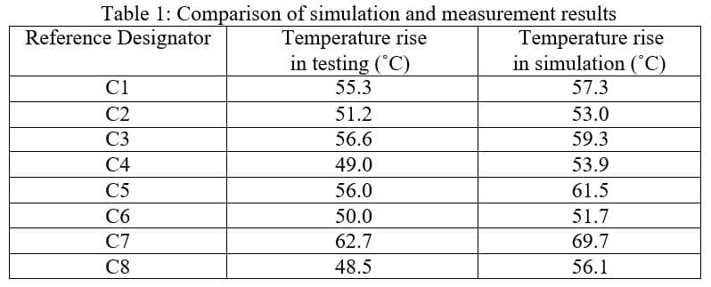
For validating the simulation results, measurement at board- and component-level is carried out in the lab via IR thermal imaging and thermo-couple measurements for thermal field and component temperature respectively. Simulation and measurement results are found to be within ± 3%. Table 1 shows the temperature of few operating components that were measured and their predicted temperature in simulation.
Base Model
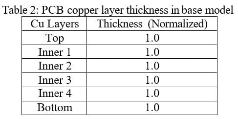
Once the simulation model is validated with the lab measurement, a full blown model is simulated with complete loading, where PCB experiences maximum current and power dissipation of the components. Copper layer thickness in the base model is considered as below:
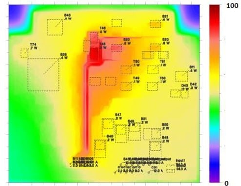
The maximum temperature rise (T) on the board is observed at 88.8 ˚C. This temperature is observed on the top side of the PCB. The total joule heating is calculated as 13.03 W.
Design Modification 1
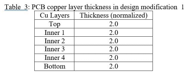
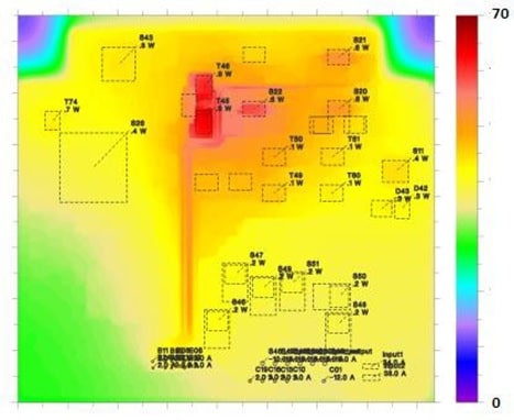
Since the Joule heating is quite high (i.e. 13 W) and contributes to heating the PCB and components, modifications are done on copper traces to reduce it. As the first step of reducing Joule heating, modifications are done to increase the cross section area of the copper trace by increasing the copper layer thickness. The copper layer thickness is considered as below:
The maximum temperature rise on board in this case is observed to be 59.8 ˚C. Joule heating reduces from 13.03 W to 6.81 W. With the increase in copper layer thickness by twice, the cross section area is increased to double. This reduces the joule heating by half.
Design Modification 2
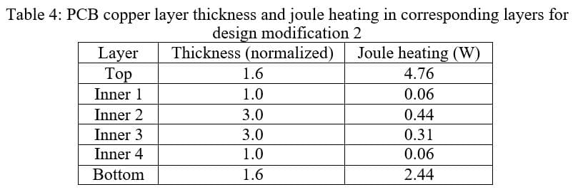
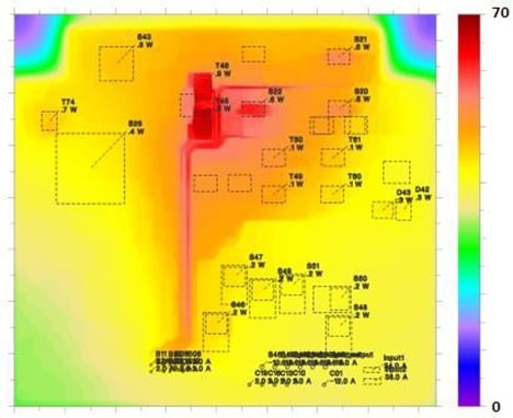
With the increase in Copper layer thickness, the cross section area increases which is an effective way of reducing the Joule heating and maximum temperature on the PCB. In the next design modification, PCB with maximum copper layer thickness available for prototyping is chosen. The copper layer thickness used is mentioned in below table.
In design modification 2, maximum temperature rise on PCB is observed as 62.5 ˚C. Total Joule heating is calculated to be 8.23 W.
Design Modification 3
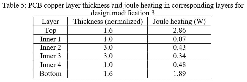
Once the PCB with maximum copper layer thickness is utilized, routing is done for increasing the current carrying traces in fourth inner layer. This leads to distribution of joule heating to inner layer. Maximum PCB temperature on board reduces by 7 K only due to distribution of current to inner layer.
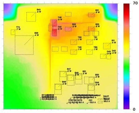
In this design, maximum temperature rise on PCB is 55.8 ˚C. Total Joule heating in inner layer 4 increases from 0.06 W to 0.48 W.
Design Modification 4
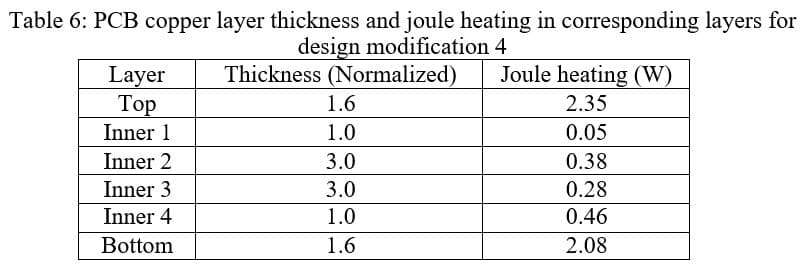
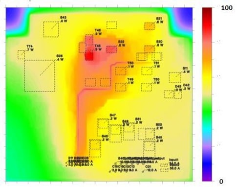
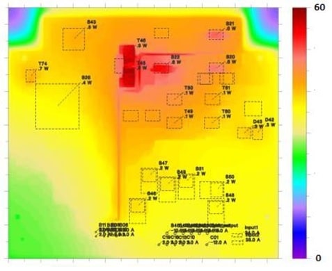
After utilizing the inner layers for carrying current, the traces with maximum current density are widened to increase the cross section. This reduces the joule heating and hence reduces the temperature on PCB.
In this case, the maximum temperature rise on PCB is observed to be 53.3˚C. Maximum current density is reduced from 140 A/mm2 to 120 A/mm2 in top layer and from 73 A/mm2 to 62 A/mm2 in inner layer 4.
Conclusion
Reduction in temperature of components and PCB is an important design goal to increase the lifetime of electronic product. To achieve the safe operating temperature on a high current density board, joule heating needs to be minimized. Reduction in joule heating is obtained through optimization of trace geometry as exhibited in design modification 1, 2 and 4. To further reduce the maximum temperature of component and PCB, inner layers are utilized to carry the current as in design modification 3.
Overall maximum temperature rise of PCB reduces from 88˚C to 53˚C, which enhances the lifetime of the electronics. This simulation also helps in identifying hot spots at early stage of development and provide measures to mitigate them.
References
- [1] Ritwik Alok Pattnayak, Laxmidhar Biswal, “Thermal design and analysis for high power automotive electronic product”, The International Conference for Engineering Analysis, Modelling & Simulation Community, NAFEMS World Congress 2015, San Diego, California 2015.
- [2] Nitesh Kumar Sardana, Ritwik Alok Pattnayak, Susyamala Pavan Kumar Busam, Chandan Kumar Ghosh, Laxmidhar Biswal, “Thermal Analysis of a Battery in an Electronic Device for an Outdoor Application”, 2016 International Conference on Electronics Packaging.

