Coauthored by: Ross Wilcoxon, Mark Dimke, Chenggang Xie
Rockwell Collins
INTRODUCTION
Die attach can play a significant role in the package level thermal resistance of wire bonded devices. Die with moderate heat flux can often be attached to the carrier substrate with organic, Silver Filled Die Attach (SFDA) materials that require relatively benign processing requirements and temperatures. However, the higher power densities seen in components such as power inverters drive designers to use materials that require higher processing temperatures, such as soldering, which can impose significant residual stresses.
Over the past decade, there has been growing use of Nano-Sintered Silver (NSS) materials that can improve thermal performance without the need for extreme processing temperatures. Studies have also shown that NSS die attach maintained lower thermal impedance[1] and higher strength[2] than soldered attach materials during thermal cycling. However, other studies have shown that the strength of NSS materials decreased by ~50% after thermal cycling[3].
This article discusses an evaluation of how thermal shock conditioning affected the thermal performance of a conventional SFDA and two commercial NSS die attach materials. The goal was to assess NSS die attach materials for use in high power electronics used in harsh environments.
TEST VEHICLE AND PROCEDURES
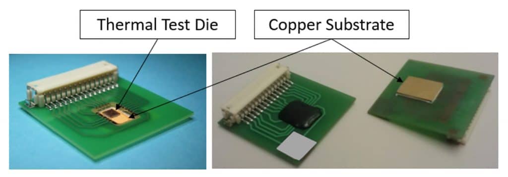
The test vehicle (Figure 1) consisted of a 25.4mm square, 0.635mm thick FR4 printed wiring board (PWB) that had a 5mm x 6mm rectangular hole milled into it. A 6mm x 10mm x 0.66mm etched copper (Cu) substrate, with electroless gold/nickel plating, was attached to the bottom of the PWB under the rectangular hole.
A 2.54mm square test die[4], which included resistive heaters and temperature sensitive diodes for monitoring temperature, was attached to the Cu substrate in the cavity formed by the hole in the PWB and the Cu substrate. Three different die attach materials were used to attach this die to the copper plate: a conventional SFDA (200°C)1 and two NSS materials, NAA1 (250°C) and NSS2 (175°C). The die was then wire bonded to the PWB and encapsulated. In all, 60 test vehicles were produced: 20 for each die attach materials included in the study.
The test vehicle thermal resistance was measured using the test fixture shown in Figure 2. This test fixture consisted of an aluminum plate with alignment posts mounted to it. A commercial thermal grease was applied to the bottom of the test vehicle copper plate prior to its being placed onto the top surface of the aluminum plate. A plastic retaining bracket with clearance holes for the alignment posts was then placed over the test vehicle A cavity on the bottom of the bracket ensured that it only contacted the perimeter of the test vehicle PWB. A 1 kg brass block, also with alignment holes, rested on the brass block to provide a retention force for the test vehicle when it was under test.
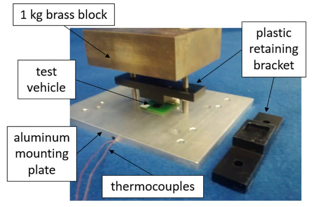
The aluminum plate was mounted to a commercial thermoelectric chiller[5]. The temperature sensitive diodes on the test die were calibrated by placing the test vehicles on the test fixture and monitoring the diode electrical resistance (with no power dissipated from the test die) over a range of baseplate temperatures. Once the diodes were calibrated, the test vehicles were powered with nominal levels of 6.8 and 15W while the aluminum baseplate was maintained at a set point temperature of 25°C. Diode resistance, voltage and current were recorded and the thermal resistance, Rthermal, was calculated using Rthermal = (Tdiode – Ttc)/(V*I), where Tdiode is the diode temperature determined using the resistance measurement and diode calibration parameters, Ttc is the average temperature of two thermocouples placed under the test vehicle and routed through a slot on the bottom of the aluminum plate, and V and I are the voltage and current supplied to the test vehicle.
Once the initial thermal resistance of all 60 test vehicles was measured, they were then subjected to thermal shock testing. This was conducted in a dual chamber thermal shock system in which samples are transferred between two temperature chambers with forced air convection. The airflow rates in each chamber were 400 SCFM (11.3 m3/min) and the chamber temperatures were set to -55°C and +125°C. The transition time between chambers was approximately 1 minute and samples were held at each temperature extreme for 15 minutes. Due to their small size, the test samples equilibrated to the chamber temperature within the first 5 minutes of the dwell. Samples accumulated approximately 40 thermal shocks per day.
Test vehicles were assigned to one of three groups that included 6 or 7 samples for each die attach. These groups of samples were periodically removed from the chamber and their thermal resistance was measured. One group was removed from the chamber 4 times during the testing while another group was removed 10 times. This was done, in part, to determine whether the thermal resistance testing process affected the results. Further details on the assembly processes, test die calibration sample test groups, testing methods, and test results are provided in Ref[6].
TEST RESULTS
Figure 3 shows the averaged package-level thermal resistance data for all components with each die attach material as a function of the number of cumulative thermal cycles. Error bars correspond to one standard deviation. These data show a relatively monotonic increase in the thermal resistance with continued thermal cycling for all of the die attach materials. The NSS 1 material did show an increase in thermal resistance at 500 cycles that appears to be due to two outlier data points in a small population.
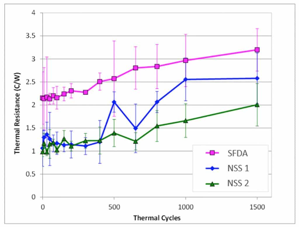
In addition, a comparison of the results for the different test groups showed that there were no significant differences in the thermal resistance of samples subjected to more thermal resistance measurements.
During the course of testing, a number of the copper substrates separated from the PWB, leaving the die embedded in the encapsulant. None of the copper substrates that lost adhesion showed any residual black encapsulant, which indicates that the encapsulant delaminated from the copper plate due to poor adhesion between the two materials. Since this failure was due to poor adhesion between the copper substrate and encapsulant, it was assumed to be unrelated to the conductive die attach materials and these failed components were not included in calculating the averaged thermal resistance results.
Figure 4 shows the cumulative copper/encapsulant adhesive failure rates for the three die attach materials. This shows that the test vehicles with the NSS 1 sintered silver die attach materials had significantly more adhesion failures than those with the SFDA die attach. The NSS 2 test vehicles were also more likely to experience adhesion failures than the SFDA, but the difference was not significant until last round of thermal shocks.

FINITE ELEMENT MODEL
The goal of the study was to evaluate how thermal shocks affected the thermal resistance effects of the die attach material. However, the testing measured the overall package thermal resistance, which included the effects of conduction through the test die, thermal spreading in the copper substrate, interface resistance between the copper substrate and the aluminum mounting plate, and spreading within the aluminum plate. To isolate the effects of the die attach, a finite element model (FEM) was created (Figure 5)[7]. This relatively simple model, with ~17,000 elements, included the test die, die attach, a copper plate, thermal grease and the aluminum plate of the test fixture. The test vehicle substrate and encapsulant were not included in the model since they played a minimal role in the thermal path for the package.
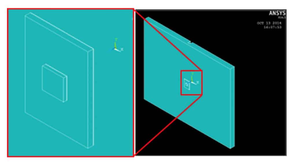
The thermal conductivity of the die attach in the FEM was varied from 2-250 W/mK while a 1W heat load was applied to the silicon. The resulting temperature drop through the package was used to determine the thermal resistance over a range of die attach thermal conductivities (Figure 6).
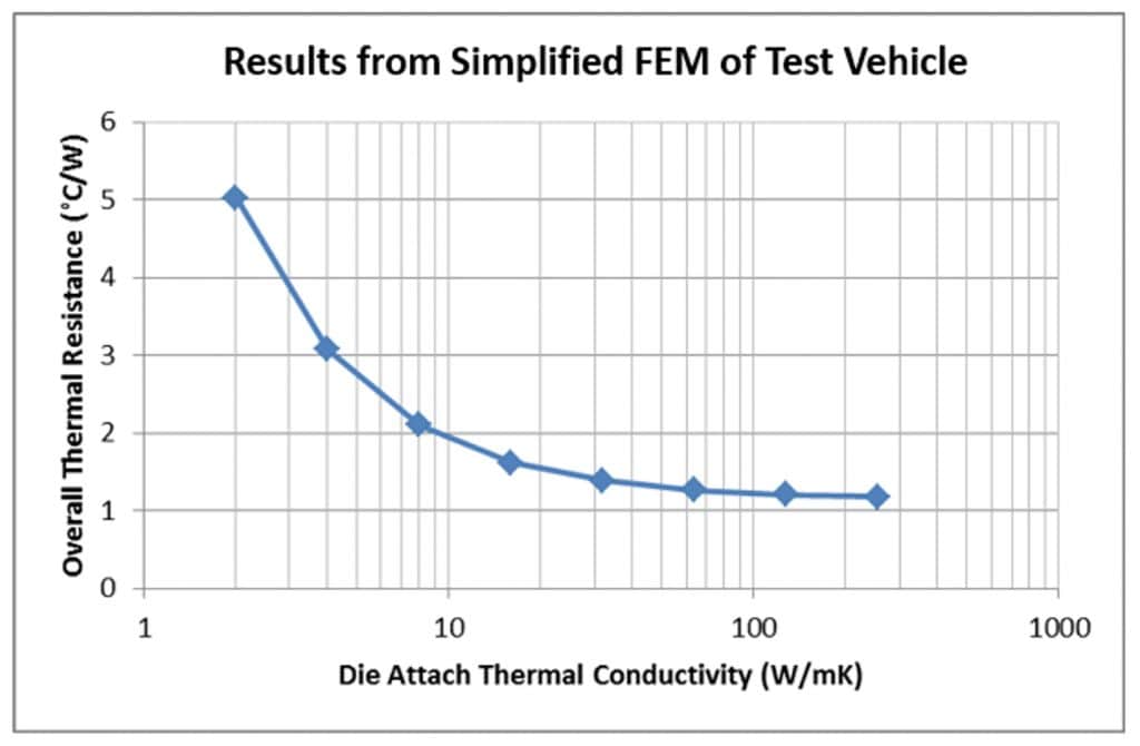
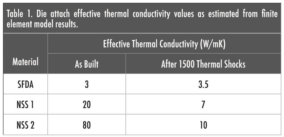
The average thermal resistance measured on the test samples with each die attach was compared to the overall thermal resistance predicted with the FEM for different die attach thermal conductivity values. This was then used to estimate the before/after effective thermal conductivity values for each die attach shown in Table 1.
DISCUSSION
The two nano-sintered silver die attach materials reduced the package-level thermal resistance compared to the baseline silver filled die attach material by approximately half. After thermal shock conditioning, the thermal resistance of all test vehicles increased, with the NSS samples continuing to show lower thermal resistance than the SFDA samples.
A simple finite element model indicated that the NSS materials initially exhibited much higher initial thermal conductivities, up to > 10x higher than the SFDA. However, based on this same model, the NSS materials degraded more significantly than the SFDA material; while the effective thermal conductivity of the SFDA material fell by over 40%, the NSS material thermal conductivities fell by nearly 90%.
Despite the more significant impact on the NSS materials, the test vehicles still exhibited lower thermal resistance after thermal shock conditioning than the SFDA test vehicles had prior to that testing. It should be noted that the degradation of the die attach thermal interface is likely much more extreme than what would occur in an actual component package, such as a Quad Flatpack No lead (QFN) device that uses a much thinner (and therefore more compliant) copper substrate.
The test vehicles with NSS die attach did experience adhesive failures between the copper substrates and encapsulant material. The root cause of these failures was not identified as part of this study. It is possible that the NSS paste may have out gassed a volatile compound that inhibited adhesion between the copper and the encapsulation that was subsequently applied to it. Further study is needed to determine if additional cleaning prior to encapsulation is required to eliminate any residual materials from the NSS.
CONCLUSIONS
This testing showed that commercially available nano-sintered silver die attach materials could substantially improve package-level thermal resistance compared to silver filled die attach. This improvement was consistent over extended thermal shock conditioning. While both commercial NSS materials in this study exhibited superior thermal performance relative to the SFDA material, one material clearly performed better than the other. In addition, test vehicles with both NSS materials were more likely to experience loss of adhesion between the copper substrate and the encapsulant than those packaged with the SFDA materials. The testing demonstrates that NSS die attach materials can reduce package-level thermal resistance as compared to conventional SFDA, but testing should be conducted to verify that the materials and the assembly processes used with them lead to components with adequate reliability for their application.
ACKNOWLEDGMENTS
The authors would like to acknowledge the contributions of Danielle Culver, Brian Otis, Roman Otterberg, Corey Bryant, Tina Berthiaume, Ken Blazek and Josh Beals.
REFERENCES
- Xiao Cao, Tao Wang, Khai D. T. Ngo, and Guo-Quan Lu; “Characterization of Lead-Free Solder and Sintered NanoSilver Die-Attach Layers Using Thermal Impedance”, IEEE Trans. on Components, Packaging and Manufacturing Technology; Vol 1, Issue 4, pp 495-501, 2011
- Li Jiang, Thomas Guangyin Lei, Khai D. T. Ngo, Guo-Quan Lu, and Shufang Luo, “Evaluation of Thermal Cycling Reliability of Sintered Nanosilver Versus Soldered Joints by Curvature Measurement”, IEEE Trans. on Components, Packaging and Manufacturing Technology; Vol. 4, Issue 5, pp. 751-761, 2014
- J.G. Bai and Guo-Quan Lu, “Thermomechanical Reliability of Low-Temperature Sintered Silver Die Attached SiC Power Device Assembly”, IEEE Trans. on Device and Materials Reliability; Vol. 6, Issue 3, pp. 436-441, 2006
- Thermal Engineering Associates TTC-1002 Thermal Test Die
- TE Technology CP-2000 HTTT Thermoelectric Chiller
- Ross Wilcoxon, Mark Dimke, Mark and Chenggang Xie; “Thermal performance and reliability assessment of nanosintered silver die attach materials”, Thermal Measurement, Modeling & Management Symposium, 31st SEMI-THERM, March 15-19, 2015, San Jose, CA
- ANSYS, Version 14.2, (simulations done in 2014), http:// www.ansys.com/

