INTRODUCTION
As integrated circuits were becoming more widespread in the 1980’s, most of the developmental problems had to do the with electrical operation of the devices and not so much on cooling them, due to low power levels. It was the electrical engineers who did the functional testing, an activity that ultimately expanded to include thermal testing. Even the thermal tests were largely an electrical exercise since temperatures were measured on silicon using diodes and elsewhere using thermocouples. The term “thermal resistance” became popular during this period when an electrical-engineer-centric culture dominated package design and development. This culture also gets credit for describing the flow state of the air when thermally testing a package in a closed box as “still air” rather than as “buoyancy-driven convection” or “natural convection”, as a thermal engineer would more accurately describe it.
Specifically, the package thermal metric, “junction-to-case thermal resistance” or ΘJC (Theta,jc) was defined and test methods prescribed at that time in Military and SEMI specifications [1]. These methods offered a choice of using either a fluid bath or a heat sink environment. They assumed that the measured ΘJC results are independent of the particular environmental heat flow conditions and that the value of ΘJC is an intrinsic property of the package, similar to the very convenient situation involving electrical resistors [1]. These beginnings in the life of the ΘJC metric apparently set the stage for confusion that continues to this day.
The rigor in thermal standards improved considerably after the founding of the JEDEC JC-15 Thermal Standards Committee in 1990. In fact, the committee charter includes the following requirements for their standards:
- These standards shall be meaningful, consistent, and shall be proven to be scientifically sound
- The standards will provide a common means of comparison of thermal phenomena for users of microelectronic packaging
During the 1990s, this committee made a significant contribution to the thermal testing of microelectronic packages by creating precise specifications for thermal test chips, test boards for mounting of a large number package types, and a variety of test environments. These environments include natural and forced convection and the junction-to-board thermal resistance conduction test environment and performing the initial work in the development of a robust junction-to-case standard [2, 3]. It should be noted that all the test boards for a particular package style are available in low- and high-conductivity versions, differing in the amount of copper in the board to control the amount of heat spreading by the board under test.
These test environments were inherently simplified, as compared with the extreme diversity of the actual application environments. Examples include the specification of a single, uniform heat source on the test die and laminar air flow in a wind tunnel. However, these simplifications made it easier for labs to implement the standards precisely and reduced the number of possible test conditions for a particular package design. This was consistent with the mission to provide a consistent basis for comparison of the thermal behavior of competing package designs.
Of course, then as now, thermal engineers are called upon not only to choose the package with the best thermal performance out of the available options, but also to predict chip temperatures in the end-use environment. In those earlier days, when thermal modeling was much less advanced, thermal engineers had to make best use of the information they had at hand. ΘJC was a convenient thermal parameter when it was necessary to estimate the temperature of a device mounted to a heat sink. Nowadays, with the availability of more powerful simulation tools and the development of more complex thermal resistance networks for representing realistic heat flows within a package, we can do much better than that [4]. Even now, there are instances when a quick, spreadsheet type network resistor model can be very useful and a ΘJC value a necessary part of the calculation.
It is possible to use the ΘJC metric intelligently, as long as the engineer understands its limitations. The next two sections are devoted to increasing the reader’s awareness of certain subtleties in measuring ΘJC and in its use in predicting chip temperatures in a package with a heat sink mounted to it. They are based on an earlier installment by this author in the column, Calculation Corner. [5]
TWO CASE STUDIES
- Simulation of ΘJC Test Environment
The junction-to-case thermal resistance, ΘJC, is calculated using the following equation, which has the same form as Ohms Law for electrical resistances:
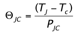
where TJ is the junction temperature (on a JEDEC-standard test chip, it is located at the top center of the chip), TC is the case temperature, normally measured at the top, center of the test package, and PJC is the dissipated power flowing from the junction to the case and then into the heat sink provided by the test apparatus. Note that PJC is normally less than the total dissipated power, PT , because usually some of the heat is lost to the environment. There are ways of determining the heat lost from the test package so that PJC can be accurately calculated [5].
The analysis below, explores the accuracy of a Finite Element Analysis (FEA) conduction model to predict the ΘJC test result for two configurations of a popular PBGA (Plastic Ball Grid Array) package.
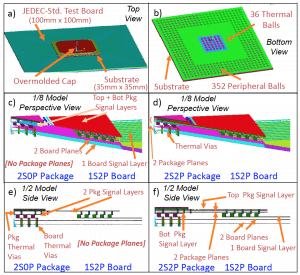
Figure 1 displays various graphics outputs from the FEA model, showing both the external and internal construction of the low-conductivity and the high-conductivity package mounted to a high-conductivity JEDEC-standard thermal test board.
Figure 1: Graphics output from FEA model showing both the external and internal construction of the package and board designs involving in this study.
Figure 2 shows temperature contour maps output by the FEA simulation involving the test package on a high-conductivity JEDEC-standard test board in the JEDEC ΘJC test environment. The stated values of ΘJC were calculated from these results using equation (1). In this manner, ΘJC was determined for the 2S0P package to be 6.2 C/W and that for the 2S2P package to be 4.8 C/W. These values compare favorably with the experimentally measured values, 6.1 C/W and 5.5 C/W, respectively. This example illustrates an important use of ΘJC test results, namely, verifying the accuracy of the representation of the internal structure of the package in the model.
Figure 2: Results of FEA thermal simulation involving low- and high- conductivity packages on low- and high- conductivity JEDEC-standard test board in the JEDEC ΘJC test environment.
- Thermal interactions between air, test board, and heat sink in wind tunnel test
This example deals with the same package design as in the previous section, but only with the 2S2P laminate configuration and with the 1S2P test board.
The analysis begins with a consideration of how to predict the junction temperature in a package with a heat sink attached to it, based on 1) thermal measurements on the package/board assembly in a wind tunnel and 2) thermal measurements made on the heat sink by its manufacturer.
The approach explored here will involve the generation of thermal resistance values for the package and board which were generated using a method described in a previous column. Specifically, the inputs to the calculation consisted of all four of the measured temperatures for the package without a heat sink (shown in Figure 3a), the total dissipated power, and the calculated heat transfer coefficient [6]. A value for ΘSA was taken from the manufacturer’s data sheet for the velocity of interest, 0.5 m/s.
Such a simple resistor-network conduction model normally accounts for heat loss to the ambient by applying a heat transfer coefficient to external surfaces assuming a global value of ambient temperature. The heat transfer coefficient can be calculated to account for buoyancy-driven convection, forced convection, and radiation heat transfer. However, it cannot account for conjugate heat transfer, in which the air flow and the subsequent transport of heat from one region to another in the model are explicitly calculated.
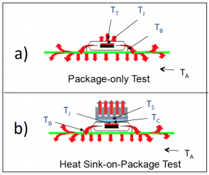
Figure 3a depicts the conduction of heat by the package and board from the chip to the ambient air. Figure 3b adds the heat sink to the top of the package. The extended area of the heat sink promotes more efficient heat transfer to the flowing air than is possible with the bare package top. However, the limitations of this simple conduction model assume that the temperature of the ambient air is not changed by the flow of heat from the solid surfaces into it. The pattern of red arrows (representing heat flow) are intended to represent this situation.
Figure 3: Diagram showing heat flow out of an arbitrary package in a wind tunnel environment as represented in a conduction model in which the loss of heat to the ambient air was accounted for using a heat transfer coefficient.
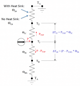
Figure 4 provides a schematic of a thermal resistor network that represents the two paths followed by the heat flow from the chip in the package. The first path is directed upward to the top of the package. The first resistor along this path is ΘJC. If no heat sink were present, the heat would then flow directly into the ambient air. The efficiency of this heat transfer process is represented by the case-to-air thermal resistance, ΘCA. If there is a heat sink present, then the heat flow through the heat sink into the air is represented by the sink-to-air thermal resistance, ΘSA. The downward flow of heat from the chip is represented by the two thermal resistances: junction-to-board, ΘJB, and the board-to-air, ΘBA. The predictions of the thermal network model for ΘJA for the package with the heat sink attached were compared to measured values of ΘJA in a wind tunnel environment.
Table 1 lists values for all of the calculated thermal resistances. The predicted value of ΘJA for the package without a heat sink present agreed very well with the measured value of 16.6 ˚C/W. This is what would have been expected and simply confirms that the calculation based on solving the thermal resistor network was working properly.
Figure 4: Thermal resistor network representing the heat flow situations in Figure 3. Note that the top resistor (terminating in the ambient air) is assigned the value of ΘCA when no heat sink is present and ΘSA when one is.
The same calculation was repeated with the exception that ΘSA was substituted for ΘCA. All the other resistor values were kept equal to those used in the calculation without a heat sink present.
The solution of the revised thermal network yielded ΘJA values that were much smaller than the measured ones. The difference was 26% for the 6mm high heat sink and 32% for the 15mm high heat sink. This indicates that the real package was running considerably hotter than that predicted by the calculation.
Why did the calculation predict much cooler chip temperatures with the heat sinks present than were measured? An explanation can be found by examining Figure 5.
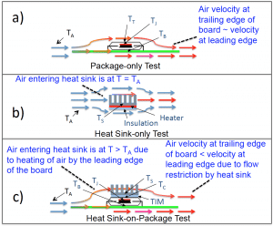
Figure 5 provides diagrams representing conjugate heat exchange with the flowing air for three test conditions involving either a) the package attached to a board or b) the heat sink with an attached heater, or c) the heat sink mounted to the package/board assembly. It indicates that in case (c), both the package/board and the heat sink are not cooled as efficiently by the airflow as when they were tested separately. This is due to a combination of preheating of the air the flowing into heat sink and to the reduction of the air velocity in the downstream half of the board.
The bottom line is that neither the board nor the heat sink are cooled as effectively when they are attached to each other compared to when they were tested separately.
Figure 5: Diagrams representing conjugate heat exchange with the flowing air for 3 test configurations involving a package/board assembly and a heat sink.
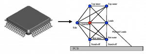
Figure 6: Drawing of a plastic leaded quad package accompanied by its thermal representation in a resistor network Compact Thermal Model generated using the DELPHI method [4]. Here the network is shown with a thermal connection to a solid entity, representing a PCB, in a CFD model. Similarly, it could be connected to a solid representing a heat sink at the top of the network.
RECOMMENDATIONS
The previous discussion made it clear that even a very simple system, such as a package attached to a board and a heat sink in a wind tunnel, cannot be accurately modeled unless the heat exchange between the solid surfaces and the flowing air is treated in a way that represents the complex physics of the heat transfer process.
However, even if the solution method accounted for this, say by using a modern computational fluid dynamics (CFD) program, there would still be problems with using thermal resistor elements that can only account for 1-dimensional heat flow. Fortunately, methods have been developed to create resistor networks that can simulate heat flows within a package representing thermal gradients that vary in three dimensions.
The JEDEC JC-15 committee has issued standards that apply what is known as the Delphi Compact Thermal Model (CTM) methodology to generate these resistor networks and integrate them into a model containing other components, such as circuit boards and heat sinks [4]. One such network is depicted in Figure 5.
The leading commercial CFD software tools serving the electronics cooling market have the capability for applying the CTM methodology. It is hoped that this article may help to raise the awareness in the industry of the benefit of applying CTM methods more widely than they are now.
The ΘJC test method still serves an important function by enabling the comparison the thermal performance of competing packaging designs related to how efficiently they transport heat to an external heat sink. Also, the correlation of a detailed simulation of a package in the ΘJC environment with the test result can serve to improve the accuracy of the thermal representation of the package internal structure in the model.
REFERENCES
[1] V.B. Dutta, “Junction-to-Case Thermal Resistance – Still a Myth?” Proceedings, 4th Annual Semi-Therm Conference, 1988.
[2] JEDEC Standard JESD51-12 — Guidelines for Reporting and Using Electronic Package Thermal Information
[3] B. Guenin, “Update on JEDEC Thermal Standards,” ElectronicsCooling, Vol, 18, No. 3, September, 2012
[4] JEDEC Standard JESD15-4 DELPHI Compact Thermal Model Guideline
[5] B. Guenin, “Use of JEDEC Thermal Metrics in Calculating Chip Temperatures in Packages with Attached Heat Sinks,” ElectronicsCooling, Vol. 20, No.1, March, 2014.
[6] J. Galloway and E. de los Heros, “Developing a Theta jc Standard Under Steady-State Testing Conditions,” ElectronicsCooling, Vol. 24, No.1, March, 2018.

