JEDEC Thermal Standards: Developing a Common Understanding
The Joint Electron Device Engineering Council (JEDEC) was established to provide recognized technical standards for a wide range of applications, from how to handle electronic packages and defining package outline drawings, to the methods used to characterize performance, including thermal. The JC-15 committee focuses on writing thermal standards to create a common reference point for generating thermal characterization data. These standards were created with the objectives that they would be meaningful, consistent, and scientifically sound. The primary purpose for adopting and following a standard is to impose a common set of testing conditions so that equivalent results will be measured when the same packages are tested by different labs. This allows end users to compare package performance from different suppliers without concern that improved performance was attributed to more favorable testing conditions. A second application for thermal standards, although often applied incorrectly, is to calculate the junction temperature for a different environment using characterization data measured under JEDEC conditions. Unfortunately, these types of calculations often lead to erroneous estimates if thermal standards are applied incorrectly.
JEDEC thermal standards continue to evolve as more complex packages and test methods are introduced. The body of work developed to date by the JC-15 committee may be organized into three distinct groups. First, standards were written to characterize thermal resistance for single die and multi-die packages. Second, thermal standards were written specifically for LEDs, accounting for the optical component of power transmission. Third, standards were written to document methods for creating simplified thermal network models that represent boundary condition independent models for electronic packages in a user-defined environment. A historical review of early JC-15 standards is documented in an earlier article [1]. More recent additions to the JC-15 standards are provided in the following sections.
1. Traditional Thermal Resistance Measurements
JC-15 thermal standards provide guidance on the steps required to perform thermal characterization tests and how to report data including chip design, board design, and testing methods. An overview of thermal standards can be found in JESD15-12. Included are definitions for thermal resistance, methods for conducting tests, and suggestions for reporting data.
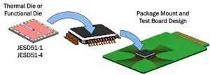
Standards were developed by documenting the steps necessary for preparing experimental test samples. These include test die and test board design as shown in Figure 1. JESD51-4 describes the requirements for implementing thermal die (either in wire bond or flip chip format) into a thermal test package.
Figure 1. Preparing a package for thermal resistance measurements.
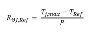
The thermal resistance is a comparative metric used to define the thermal performance of a package for a given testing environment. It is defined as the maximum die temperature, ????????,????????????, increase above the local reference temperature, ????????????????, per unit of power applied, ????, see equation (1). A lower resistance package will respond with a lower temperature difference compared to a higher resistance package for the same power input.
(1)
Note that the TRef is the cooling reference condition. It could be the ambient air, TA, the package case surface, TC, cooled by an external heat sink, or the board temperature, TB, when cooled by a heat sink mounted to the perimeter of the test board.
Thus equation (1) represent three different thermal resistances; RΘJA , RΘJB, or RΘJC, depending on the cooling environment. Heat is removed from the package by conduction when the package makes direct contact with a heat sink, TRef = TC or TRef = TB, or indirectly by convection and radiation, TRef = TA.
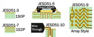
Depending on the style of the device under test, DUT, various test board designs are required to make electrical connections, either lead frame or ball array style. Several JEDEC standards were written to document test board designs for different testing conditions as shown in Figure 2.
JEDEC test boards are relatively large, at least 76 mm x 114 mm and have thick copper on the top trace layer, at least 50 um. They are sized accordingly to reduce the variability in thermal resistance measurements caused by variations in board fabrication, e.g. trace thickness variation.
Figure 2. Board style.
An upper bound estimate on thermal resistance is made by testing packages on boards having only top layer signal traces without any internal planes (1S0P). Board design details are specified in JESD51-3. This is appropriate for applications where the test board does not have extensive power and/or ground planes, and the primary conduction path away from the package is through the traces on the top layer. When power and ground planes are included in the board, single layer traces on top layer with 2 internal planes (1S2P), the additional copper planes provide a conductive path to remove heat from the package. Test board design details for 1S2P are found in JESD51-7. In general, a 1S2P board will produce a junction-to-ambient thermal resistance, RΘJA that is approximately 50% less than that measured using a 1S0P board. When thermal vias are added to the 1S2P boards, making a direct path from the package to the ground plane, the thermal resistance is reduced even further. A description of the via pattern and sizes for the thermally enhanced test board design can be found in JESD51-5.
JESD51-10 provides direction for designing test boards for wire-through leaded packages. Lastly, for array style packages, including ball grid array, BGA, style packages, JESD51-9 provides guidance on test board trace fan out designs.
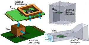
The environmental test conditions are described in separate standards for each type of thermal resistance. These include conduction-based tests to measure the junction-to-board resistance, RΘJB,
and the junction-to-case resistance, RΘJC, as shown in Figure 3. JESD51-8 defines the conditions necessary for measuring RΘJB including the design of a double ring cold plate.
Figure 3. JEDEC-standard environments for running thermal resistance tests.
Developing a reliable method for measuring RΘJC has been a challenge due to the difficulties in accurately measuring the case temperature without influencing the heat flow path and providing a cold plate design that does not greatly impact RΘJC measurements. A steady-state RΘJC standard has been in the development stage for some time. However, limited progress has been made due to the complexities of measuring the case temperature without affecting the conductive heat flow path [2].
JESD51-14 provides a clever way for extracting RΘJC without requiring the measurement of the case temperature. It does so by making high-speed transient temperature measurements (e.g. 1 MHz) in order to capture early temperatures just as the power is turned off. At very small values of elapsed time after the power is turned off, the thermal wave has not exited the package case, and is therefore insensitive to cold plate design effects. By making two measurements, one with good thermal contact with the heat sink and a second with a thin insulator between the package and the cold plate, one can compare the two curves to arrive at an estimate for RΘJC. This method should only be applied when there is one heat flow direction, e.g. die is mounted to a copper heat spreader, and should not be used if there is significant lateral heat spreading in the package.
The other two resistance, RΘJA for natural convection and RΘJMA for moving air, is shown in Figure 3. An upper bound resistance is determined for natural convection cooling using JESD51-2. The test board is inserted inside a 0.3 m x 0.3 m x 0.3 m. Weak buoyancy induced flow, caused by the heated test board and package, create a controlled natural convection boundary condition that is insensitive to external disturbance in the testing lab. For wind-tunnel testing with forced convection flow, lower resistances, RΘJMA, are observed. A summary of conditions for testing DUTs under forced convection flow is found in JESD51-6.
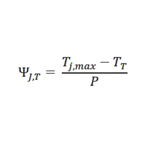
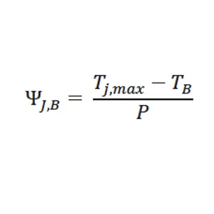
Parameters, ΨJT and ΨJB introduced in equations 2 and 3 represent the junction temperature rise compared to a local referenced temperature either measured on the top of the package, TT, or on the board, TB, at a location 1 mm from the edge of the package. ΨJT and ΨJB measurements made during JEDEC natural convection and moving air tests, JESD51-2A and JESD51-6, can be used to estimate the junction temperature with reasonably accuracy for packages mounted in a non-JEDEC environment, e.g. on functional boards.
(2)
(3)
By mounting a thermocouple on top of the package and measuring TT in the actual application, one can estimate the junction temperature as ????????,????????????= ΨJT* P + TT. Similarly, if a thermocouple is mounted 1 mm from the edge of the package, one can estimate the junction temperature as ????????,????????????= ΨJB* P + TB. Package vendors typically supply data for both ΨJT and ΨJB as a function of local air velocity.
The earlier package thermal test standards were developed for a single die. Hence data reporting was rather straightforward. Extension of single die package standards were made in JESD51-31 to include methods for reporting data for multi-die packages. In addition, suggestions were provided on methods for sensing the case temperature at multiple locations. The board design as outlined in previous standards became limited by the smaller number of edge connector leads available as more traces were required to support multi-die packages. JESD51-32 provides an extension to board design when the trace number becomes limited by the previously constrained connector design.
2. LED Thermal Standards
Thermal standards have evolved as new electronic package styles have been developed. For example, just 15 years ago, light emitting diodes (LEDs) where not commonly used for room illumination in residential and commercial applications. As new products are introduced, thermal standards must adapt to accommodate the latest advances in technology.
The characterization of LEDs are more challenging than electrical only packages because of the additional energy component due to light. A new series of thermal standards were written to describe conditions necessary for performing electro-optical measurements of LED packages. JESD51-50 provides an introduction to LED measurements including a description of the method to subtract the optical power from the electrical power to determine the dissipated thermal power. Details for measuring thermal resistance of LEDs are discussed in JESD51-51. JESD51-52 describes methods for measuring the optical power using an integrating sphere. More parameters are required to define the thermal resistance of LEDs than traditional packages. A summary of thermal characterization terms for LEDs are compiled in JESD51-53 and can be used as a convenient reference guide.
3. Simulation Based JEDEC Standards
It is tempting for many users to apply JC-15 thermal resistances, as supplied by package vendors, directly to predict the junction temperature while operating in a totally different system environment. Although this may be convenient since the data is readily available, the predictions cannot be expected to be accurate for different environmental conditions or for different test board design. An alternative method was needed to allow users to predict junction temperature in environments different than the standard JEDEC thermal environment. Compact thermal models were introduced as an approximation modeling method to predict junction temperature in a non-standard JEDEC environment. A compact thermal model is a simplified resistor network that approximates the three-dimensional heat conduction problem [3]. Typical electronic package.
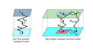
JESD15-3 provides a description of the two-resistor thermal model.
Although the two-resistor model is quite simple, it can produce errors as great as 30% depending on the environmental conditions present in the actual system. By adding more external areas, nodes and resistors, the accuracy improves dramatically. A DELPHI [4] compact thermal model, CTM, has inner and outer areas on the top and bottom surfaces, JESD15-4. More resistors can be added to accommodate the non-isothermal areas present in the actual package. Quite often two more resistors are added to CTMs between nodes TJ and TBO and between TJ and TTO. Numerical values for resistors are adjusted so that the network model agrees with the detailed model over a wide range of boundary conditions applied to the external areas. Theoretically, it is possible to add even more nodes and resistors to the point where the model exactly represents the temperature field in the FEA model. Realistically, as more nodes are added to the model, the effort required to generate resistance values becomes exponentially more difficult. A CTM typically agrees with a detailed model for a customer environment with a difference less than 1%. These models are said to be boundary condition independent (BCI). Users can apply CTMs with confidence that they will accurately predict junction temperatures in a custom user environment. JESD15-4 provides a standard for implementing DELPHI CTMs. Notice that the standard is written for predicting steady–state conditions. CTMs can be extended to predict transient conditions by adding “thermal” capacitors between individual nodes the ambient node, see for example [5].
A more efficient means is necessary to transmit resistances, areas, and nodal topology from the package vendor to the end–user. A simple data sheet with printed numerical values is too cumbersome for exchanging model data for CTMs. A more efficient method was created using an electronic data sheet written in an eXtensible Markup Language (XML). JEDEC standard JEP 30-A100 and JEP 30-T100 provide a summary of the format used to document CTM models. A definition file, called a schema, is available on the JEDEC website that will provide a starting point for documenting CTMs.
With the introduction of two-resistor and CTMs, the end user can create accurate system level thermal models for steady-state and transient conditions with one caveat. It is best used for package with a single die. There are methods for creating CTMs for multi-die packages but the optimization problem becomes extremely difficult and cannot in general be applied reliably for all types of packages and conditions. The prevailing trend in package design is to include more heat dissipating die into individual packages called multi-chip modules, MCMs.
To overcome this difficulty, a totally different approach was taken by the package simulation software vendors. Rather than rely on a resistor/capacitor network with a physical structure, a reduced order model, ROM, was developed. A good overview of ROMs can be found in [6] and [7]. Currently there are no JEDEC standards for ROMs. However, due to the popularity and availability of simulation software to generate ROMs, new standards will be required to provide a common framework for exchanging data between package suppliers and system designers.
The JC-15 thermal committee continues to support new thermal standards that respond to changes in package styles and methods for generating thermal models. All JEDEC standards referenced here can be downloaded free of charge by accessing the given URL [8] with the specific standards number of interest. Meetings are held three times a year and are open to JEDEC members and the general public. A meeting schedule for JC-15 can be found on the JEDEC website, www.jedec.org.
References
[1] Guenin B., “Update on JEDEC Thermal Standards”, Electronics Cooling, September, 2012. https://www.electronics-cooling.com/2012/09/update-on-jedec-thermal-standards/
[2] Galloway J., “Developing a Thetajc Standard Under Steady-State Testing Conditions”, Electronics Cooling, Spring, 2018, https://www.electronics-cooling.com/2018/03/developing-thetajc-standard-steady-state-testing-conditions.
[3] Lasance C., “Ten Years of Boundary-Condition- Independent Compact Thermal Modeling of Electronic Parts: A Review”, 2008, Journal Heat Transfer Engineering Volume 29, - Issue 2.
[4] Rosten H., Parry J., Lasance C. J. M. et al, “Final Report to SEMI-THERM XIII on the European-Funded Project DELPHI – The Development of Libraries and Physical Models for an Integrated Design Environment,” Proc. of the Thirteenth IEEE SEMI-THERM Symposium, Austin, TX USA, January 28-30, 1997.
[5] Sabry M.N. and Dessouky M., “A framework theory for Dynamic Compact Thermal Models”, 2012 28th Annual IEEE Semiconductor Thermal Measurement and Management Symposium (SEMI-THERM)
[6] Bechtold T., Rudnyi E.B., Korvink J.G. (2008) Model Order Reduction for MEMS: Methodology and Computational Environment for Electro-Thermal Models. In: Schilders W.H.A., van der Vorst H.A., Rommes J. (eds) Model Order Reduction: Theory, Research Aspects and Applications. Mathematics in Industry (The European Consortium for Mathematics in Industry), vol 13. Springer, Berlin, Heidelberg.
[7] Codecasa L., d’Alessandro V., Magnani A., Rinaldi N., Zampardi P., “Fast novel thermal analysis simulation tool for integrated circuits
(FANTASTIC)”, 2014, 20th International Workshop on Thermal Investigations of ICs and Systems.
[8] JEDEC standards document download, https://www.jedec.org/standards-documents/
