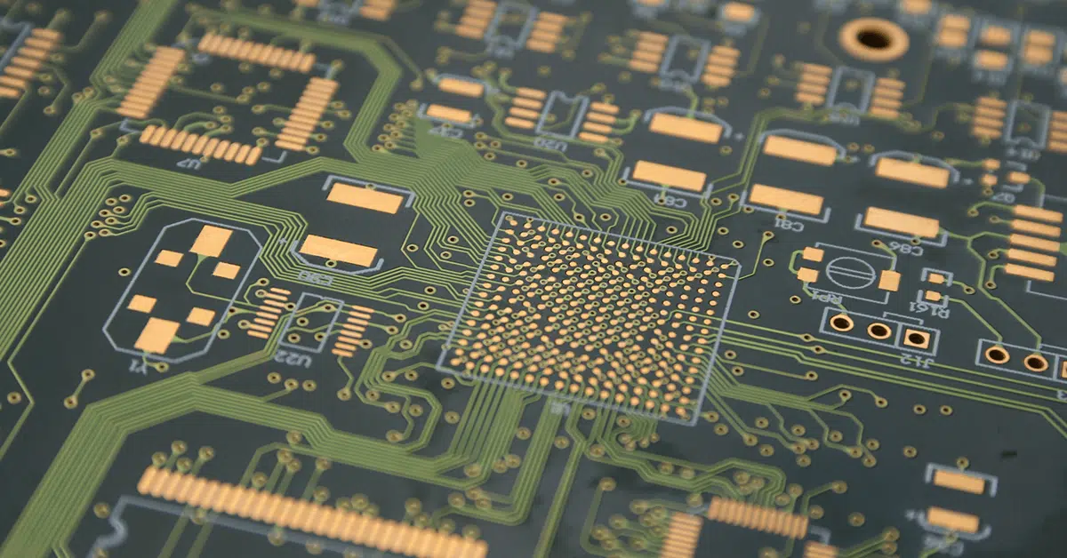
PCB Fabrication is the process of building a physical PCB from a circuit board design by following the prescribed set of specifications. The understanding of the design specifications is very significant as it affects the PCB’s manufacturability, performance, and production yield rate.
One of the vital design specifications to be followed is the ‘copper balance’ in the PCB Fabrication. The consistent copper coverage in each layer of the PCB stack-up has to be achieved to avoid electrical and mechanical issues that can impede the circuit performance.
Copper balancing is a method of symmetric distribution of copper traces in every layer of the PCB stack-up. This is necessary to avoid concerns of board twists, bow, or warpage. Layout engineers and fabricators insist on the mirrored stack up with the top half layers to be exactly symmetric with the bottom half layers of the PCB.
Copper is an integral part of any PCB design as it has exceptional electrical and thermal characteristics necessary for signal transmission and heat dissipation.
- Copper used as traces transfer heat along with signal across the board. This decreases the damage caused by irregular heating of the board that may lead to internal track breakage.
- Copper used as a heat sink layer for power generating circuits avoids the usage of extra heat sink components and reduces the manufacturing costs to a good extent.
- Copper used as a plating on the PCB increases the conductor and surface pad thickness. Also, a strong inter-layer copper connection is achieved through plated through holes.
In PCB Fabrication, if there is an uneven distribution of copper among the stack-up layers then the following mechanical alignment issues can occur.
- Twists: The vertical displacement of one corner that is not in the same plane as compared to the remaining three corners of the board is known as the twist in the PCB.
- Bow: A spherical or cylindrical curvature of the PCB while the four corners of the board are in the same plane is said to be the Bow issue of the board.
- Warp: Any unintended change in the PCB shape is known as Board Warping in general. The high temperature and pressure of the fabrication process itself can cause warpage which is also known as the “Potato chip” effect in PCB Fabrication. The warped boards can stress the traces or solder joints which might further lead to damaged circuits.
Bow and Twist issues also depend on the technical characteristics of a PCB like board thickness, type of substrate materials, etc. Thin boards get warped frequently while going through high-temperature fabrication processes. Selecting the right type of material and correct PCB thickness can help in reducing the mechanical issues to a good extent.
PCB Copper balance plays a significant role in PCB fabrication and component assembly. Even distribution of copper in each layer and across the entire stack up is important to avoid issues of the bow, twist, and warping of PCB.
If stack-up is not balanced, along with bow and twist issues there can be variation in the overall PCB thickness. Uneven copper coverage in different layers can lead to mismatched thickness on each side of the board after the lamination process.
So, the goal here is to eliminate the areas that could deform the board when subjected to the pressure of the production process. Any deformed board causes serious trouble while component assembling, even worse if it is on an automated assembly line with pick and place technique.
Let’s see how we can achieve copper balance during the circuit design stage to further manufacture PCBs with the best yield:
- During the stack-up design, it is advised to set the central layer with a maximum copper thickness and further balance the remaining layers to match with their mirror opposite layers. This recommendation is important to avoid the potato chip effect discussed earlier.
- Where there are wide copper areas on the PCB, it’s wise to design them as grids instead of solid planes to avoid the copper density mismatch in that layer. This avoids the bow and twist issues to a great extent.
- In the stack up, the power planes should be placed symmetrically and the copper weight used in each power plane should be of the same quantity.
- Copper balance is necessary not only in signal or power planes but also in the core and prepreg layers of the PCB. Ensuring a uniform copper proportion in these layers is a great way of maintaining overall PCB copper balance.
- If there is an excess copper area in a particular layer then the symmetrically opposite layer should be filled with tiny copper grids to balance out. Those tiny grids of copper will not be connected to any net and will not disturb the functionality. But it is necessary to ensure that there is no impact on the signal integrity or the board impedance due to this copper balancing technique.
Achieving copper balance in PCB design can provide more benefits than just reducing the board warpage (Bow, Twist, Sag, etc.) issues. Copper balance ensures uniform copper plating across each PCB layer. This further creates consistent conductor thickness on the plated surface improving signal transmission and overall circuit performance. Also, PCB copper balance results in consistent PCB thickness during lamination. It further reduces possible low-pressure areas that may result in fabrication issues calling for re-design. Thus, PCB copper balance serves a vital role in the PCB fabrication process.


