Introduction
The growth of battery powered applications is presenting new challenges for designers of electronic motor-driven solutions. Targeting higher performance and efficiency, the power stages of these products must manage high currents while meeting strict power dissipation and size requirements. This article illustrates a thermally aware workflow with Cadence® Celsius™ Thermal Solver technology that was used by STMicroelectronics, a leading manufacturer of industrial motor control integrated circuits (ICs), to optimize the EVALSTDRIVE101 evaluation board deployed in battery powered electronics.
The Celsius Thermal Solver is a complete electrothermal co-simulation solution for the full hierarchy of electronic systems from ICs to physical enclosures that enables deeper system analysis and design insights and empowers electrical design teams to detect and mitigate thermal issues early in the design process, reducing electronic system development time. The Celsius solver integrates with Cadence IC, package, and PCB implementation platforms and leverages a massively parallel architecture for 10 times faster performance than legacy solutions without sacrificing accuracy.
The software provided detailed electrothermal co-simulations during the routing phase, enabling the STMicroelectronics designer to achieve maximum system performance in a short timeframe.
Thermal Design Challenges
The use of batteries for application power supplies requires lower operating voltage, usually in the range of a few tens of volts, due to the limited number of battery cells connected in a series. When applications require high power above hundreds of watts, the management of currents flowing through the motor driving the electronics becomes critical to ensure overall system efficiency and reliability. Indeed, motor currents may exceed tens of amperes in such applications, which leads to increased power dissipation inside the inverter module, reducing its efficiency. More power to the electronic components of the inverter also results in higher temperatures, which could consequently degrade their performance over time and/or cause sudden breaks if going above maximum allowed ratings.
Several electronic components widely used in motor control systems are very sensitive to operating ambient temperature. For example, electrolytic capacitors typically used to stabilize the main supply voltage of the inverter are guaranteed by the manufacturer for a minimum number of hours without failures if their temperature remains below specific thresholds, but if operated above the threshold a reduction of their average life should be expected.
Consequently, the optimization of thermal performance, in combination with a compact form factor, is a key aspect of the inverter design phase that can hide pitfalls if not properly addressed, resulting in underperforming products.
The current density in the PCB is also a critical factor when the current flows between different planes through via holes. Overstressing a single via connection due to poor placement could result in a sudden failure during operation, making analysis of this issue critical as well. A traditional approach to this problem would typically be the production of a first prototype once electrical signoff is completed and a direct check of its thermal performance by on-field validation. The design would then be successively refined, and new prototypes evaluated again in an iterative loop that should converge to the optimal result. The problem with this approach is that electrical and thermal evaluations are totally separated, and electrothermal coupling effects are never addressed during PCB design process, resulting in a long iteration time that directly impacts the time to market.
A more effective alternative method is to optimize the electrothermal performance of motor control systems by taking advantage of modern simulation technologies. This article describes how STMicroelectronics fine-tuned its EVALSTDRIVE101 evaluation board using the Celsius Thermal Solver, which provided in just a few minutes a global and accurate assessment of design performance from both an electrical and thermal perspective. This tool dramatically simplified the inverter optimization process and enabled the designers to achieve a compact and reliable design in a short timeframe.
The EVALSTDRIVE101 Demonstration Board
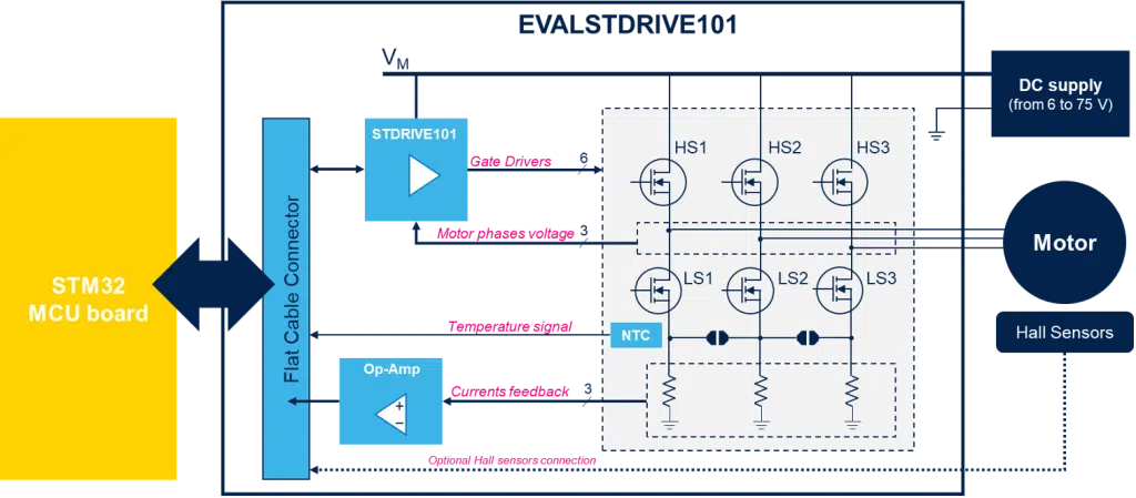
The EVALSTDRIVE101 is a high-power demonstration board designed to drive three-phase brushless motors. It is based on the STDRIVE101 three-phase gate driver, and six STL110N10F7 power metal-oxide semiconductor field-effect transistors (MOSFETs), arranged into three half bridges. The block diagram of the EVALSTDRIVE101 is represented in Figure 1.
Figure 1: EVALSTDRIVE101 basic block diagram
From a thermal perspective, the most critical part of the EVALSTDRIVE101 is the power stage area that mainly includes power MOSFETs, shunt resistors, ceramic bypass capacitors, electrolytic bulk capacitors, and connectors. The layout of this part of the board, seen in Figures 3-6, covers roughly half of overall PCB size, i.e., 50cm2. Special care was taken in the placement and routing of the MOSFETs since these components are responsible for most of power losses during inverter operations.
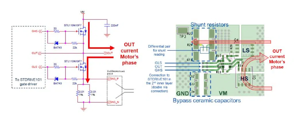
In addition to the thermal perspective, the PCB routing also optimizes electrical performance. The lower panel of Figure 2 shows a placement detail of one half bridge; the MOSFETs, shunt resistors, and ceramic capacitors were placed close each other to minimize current loops and were connected by large top traces to reduce inductive and resistive components positively affecting radiated emission and noise level. The same reduction of parasitics was implemented for connections between STDRIVE101 gate driver and MOSFETs using incremented width of 0.7mm and two vias for each crossing of layers. This, together with a tuned polarization network of MOSFET gates made by a 33Ω resistor in parallel with a Schottky diode (shown in the upper panel of Figure 2) also allowed the designer to control the induced turn on effects and obtain the best motor control.
Figure 2: Schematic of one-half bridge in the EVALSTDRIVE101 and associated layout pattern
Thermal Analysis and Optimization
Critical points in the current flow that could produce overstress of the EVALSTDRIVE101 board were identified using the Celsius Thermal Solver, which enabled the designers to perform an electrical analysis of the system that provided current densities in traces and vias, as well as voltage drops. These kinds of simulations require designers to define the PCB’s current loops of interest using a circuit model for the system, made of current sinks, voltage sources, and resistances.
Current paths are not immediately defined for the inverter since these depend on operating condition of the three half bridges. A full description of system behavior should include current exchange through the high-side or low-side MOSFET within one PWM cycle and account for realistic motor driving by amplitude modulation over time. However, it would be overdetailed and of little use for a simulation that is intended to address longer time-scale phenomena. A more convenient representation is proposed in Figure 3 for each half bridge. It consists simply of two constant current generators placed between the output and power supply connectors and three short circuits modeling the MOSFETs and shunt resistor. The two current loops provide a good fitting with real case average currents throughout the supply rail and ground plain while the output path current is slightly oversized, a convenient operating condition for evaluating design robustness.
Figure 3: PCB current loop modeling
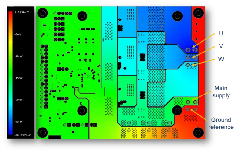
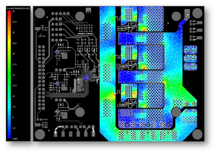
Figures 4 and 5 show the voltage drops and current density of the EVALSTDRIVE101 with 𝐼𝐿 of 15A. Voltage drops simulated with the Celsius Thermal Solver with respect to ground reference highlight a particularly optimized layout with an absence of bottlenecks and well-balanced outputs at 28 mV, 25 mV, and 23 mV for U, V, and W. Output U shows the highest voltage drop while output W, the lowest of the three, that is an expected result considering relative path lengths from power connector.
Figure 4: Voltage drops resulting from DC current loops
The Celsius Thermal Solver analysis of current distributions also confirmed the board’s targeted performance (Figure 13). The currents are well distributed in the various paths and have an average density below 15A/mm2, which is the recommended value for power traces sizing. Some red areas are highlighted in the proximity of the MOSFETs, the shunt resistors, and the connectors. These represent a higher current density, due to components’ terminals smaller than the underlying power traces. However, the maximum current density is far below the limit of 50A/mm2, which could realistically lead to reliability issues [1].
Figure 5: Current density resulting from DC current loops
The designers used the Celsius Thermal Solver to set up and run steady-state or transient simulations for thermal analysis. The former provides a single 2D temperature map for layers and components, while the latter provides maps for each simulated time instant and warmup curves at a cost of longer simulation time. Settings needed for steady-state simulation can be applied to a transient simulation, but this additionally requires a definition of power dissipation functions for the components. Transient simulations are suitable when defining different operating states for the system with power sources not simultaneously active and also to assess the time needed to reach steady-state temperature. Simulations were done at an ambient temperature of 28 °C with the heat transfer coefficient as boundary conditions and two-resistors thermal model for devices. These models were used instead of detailed thermal models like Delphi since directly available in components datasheets although slightly sacrificing the simulation accuracy [2]. The power loss of the inverter was estimated by simplified formulae considering contribution of shunt resistors and power MOSFTEs due to conduction, switching and diode’s drop.
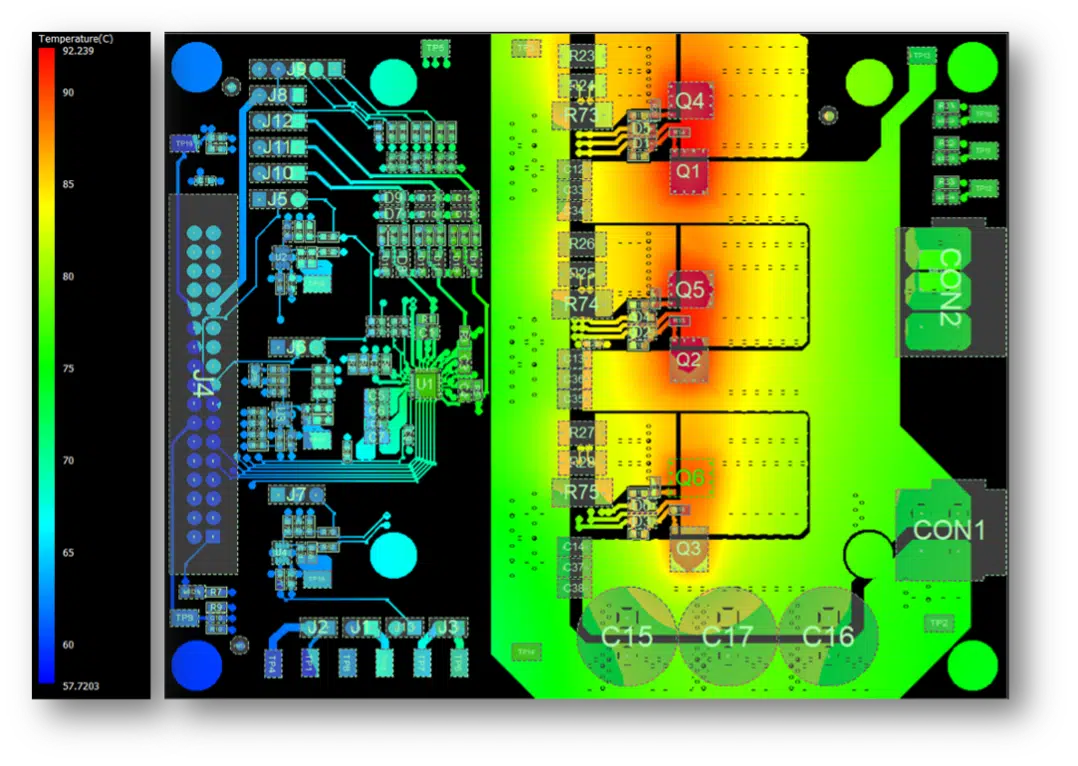
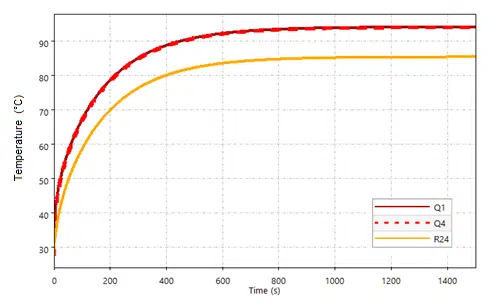
Steady state results for the EVALSTDRIVE101 are provided in Figure 6 and transient simulation results in Figure 7. Step power functions are used in transient simulation to enable all the MOSEFTs and the shunt resistor at time zero.
Figure 6: Simulation results showing steady-state PCB simulated top layer temperature map
Figure 7: Simulation results showing component warmup of the U half-bridge simulated thermal transient curve
From the simulation results, the Q1 MOSFET was the hot spot on the board, at 94.06°C. Other components such as the Q4 MOSFET at R24 and R23 had a temperature of 93.99°C, 85.34°C, and 85.58°C, respectively.
Thermal Characterization: Simulation versus Measured Data
For the thermal performance evaluation of the EVALSTDRIVE101 board, a setup was used consisting of three coils wired in a star configuration, namely a three-phase load that emulates the motor. Each coil must have a saturation current compatible with the board rating, but the inductance or its parasitic resistance value does not need to be equivalent to that of emulated motor. Indeed, it is more advantageous to have low parasitic resistance value for the coils, to considerably reduce the active power that would lead to unnecessary Joule effect heating inside the coils and obtain a lossless reactive power transfer between the board and the load and vice versa.
By applying three sinusoidal voltages that are out of phase by 120° to each other to the three terminals of the load, the three sinusoidal currents flow in the load. The three sinusoidal outputs are generated by modulating the PWM duty cycle around 50% mean value as in SV-PWM.
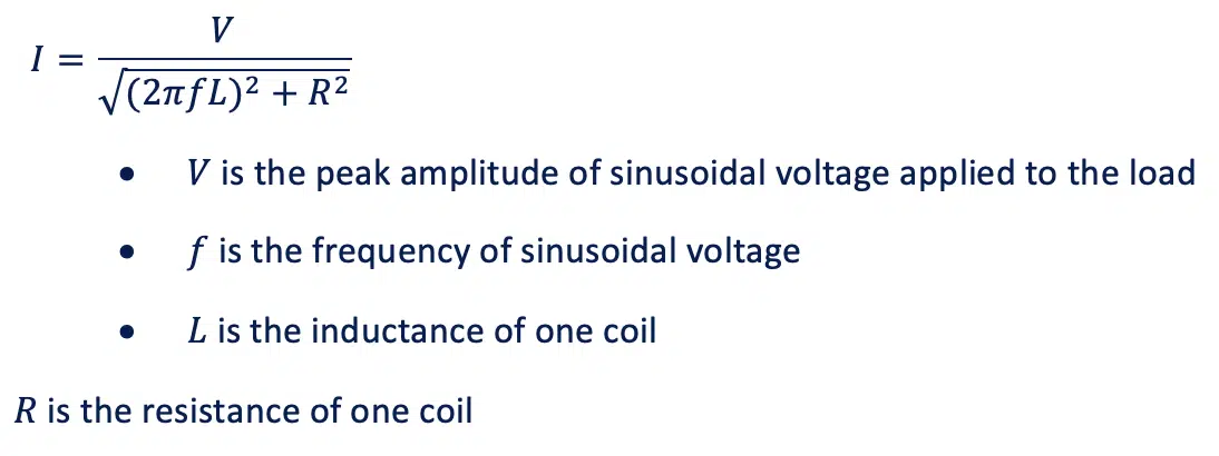
The peak amplitude of the current is obtained by:
Equation 1
With this method the power stage works in an operating condition very close to the final motor driving application. Furthermore, the load current is stable and easy to configure by simply varying the frequency and applied voltage amplitude conversely to the motor driving, which needs appropriate closed-loop control algorithms.
The device was connected to a control board to generate the necessary driving signals and is placed inside a plexiglass box to obtain system cooling by convection without accidental air flow. Above the box there is one thermal imaging camera, which frames the board through a hole in the cover of the box.
A three-phase load with inductance of 300µH and resistance of 25mΩ for each coil is connected to the board outputs, as previously described, and 36V is supplied to the system. An output current of 15Arms was obtained by applying three out-of-phase sinusoids with a frequency of 100Hz. The PWM applied by the half-bridges has a frequency of 20kHz and a dead time of 500ns.
Power Loss Measurement
One factor affecting the quality of the simulation results is certainly the data accuracy of the power dissipated by each device on the power stage. Measurement was made on the board as described below to evaluate the error in quantifying the dissipated power.
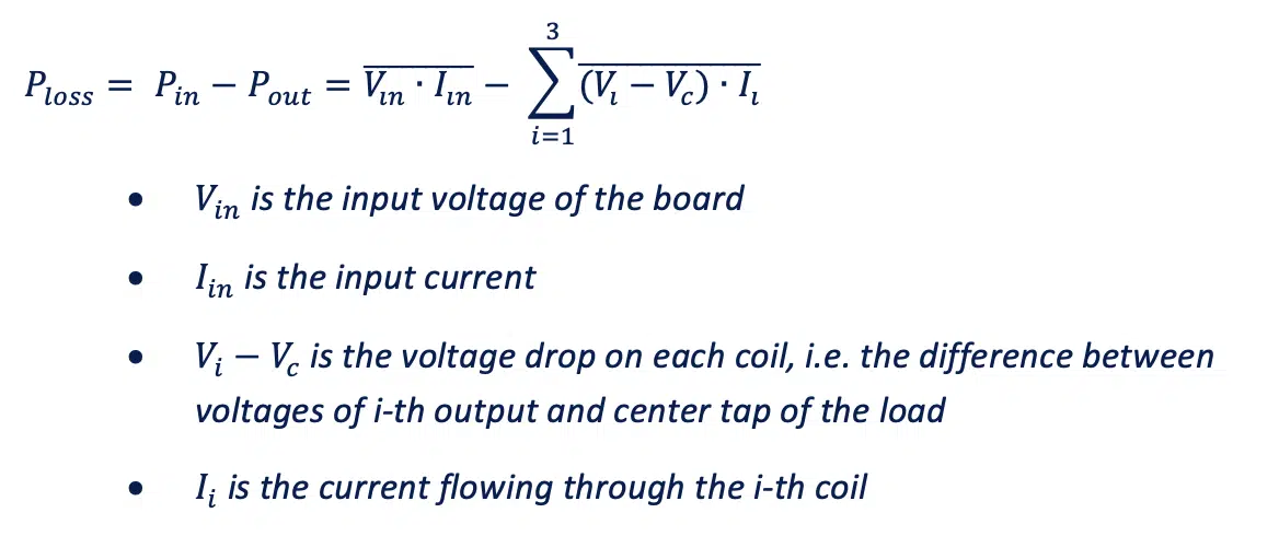
Since the power dissipated by the board is the difference between the input power and the power delivered to the output load, it can be calculated using following equation:
Equation 2
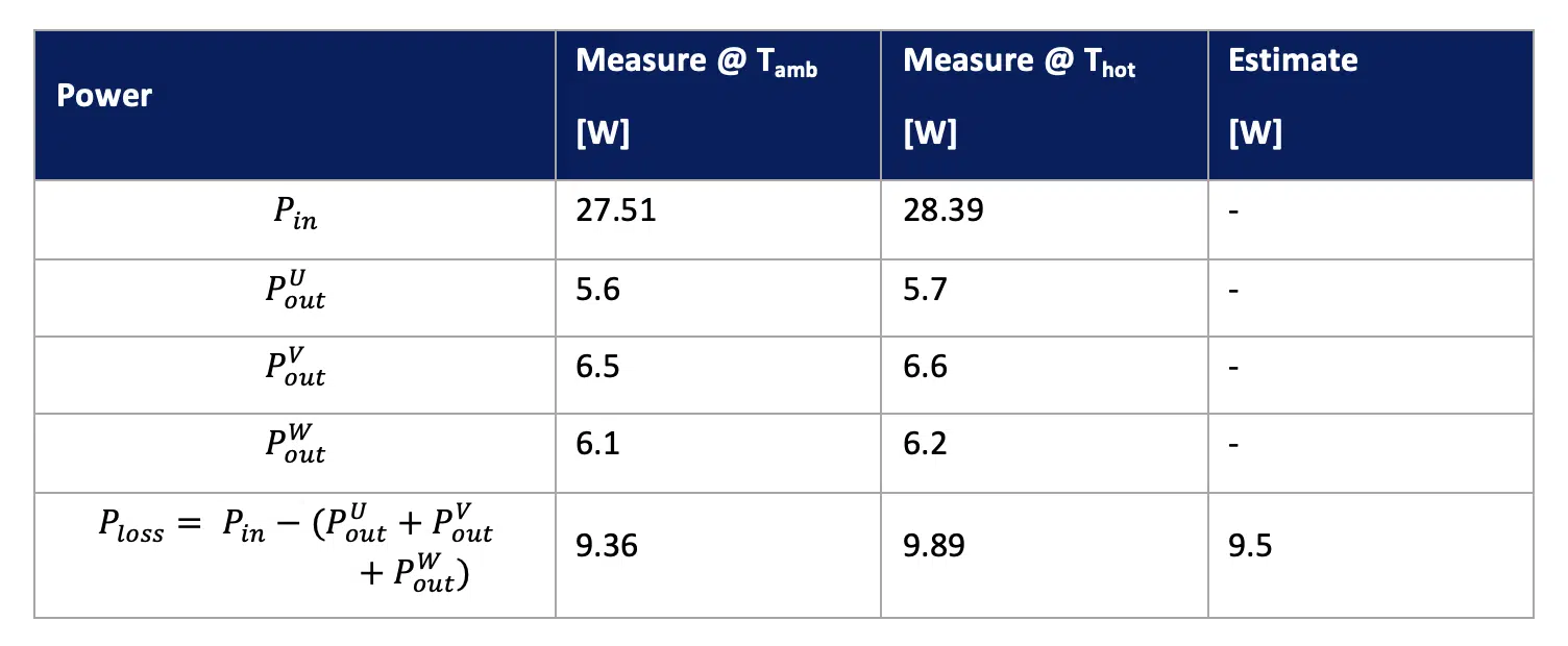
The measurement was made using an oscilloscope and applying the proper math functions to the waveforms: first the point-by-point product of the voltage and current was computed, then the power was averaged over an integer number of sinusoid cycles. Table 1 shows the measurement results at ambient temperature and at hot when the power stage reached steady state condition. The overall value of power dissipated by the board estimated by formulae is also provided.
Table 1: Measured vs. estimated power losses
The results show a very good matching between measurements and estimates which is in line with introduced approximations. An overestimation of the measurement at room temperature of 1.5% is made by the formulae, which provides roughly a 3.9% underestimate compared with hot condition data. This result is in line with the variability associated with the on-resistance of the MOSFETs and shunt resistors since nominal values were used in the computations.
As expected, all power values were higher at hot than at room temperature, due to the increase of the resistances of the coils and MOSFETs with temperature. The data also shows a difference among the measured powers for the three outputs. This effect is due to the unbalancing of the three-phase load, because of slightly different values of L and R from coil to coil. This effect plays a marginal role, since the misalignment is lower than the one between the measurements and the estimate.
Temperature Results
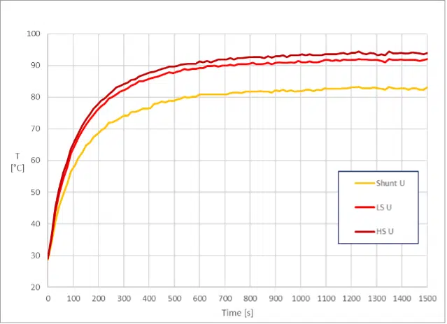
The sinusoids generation and acquisition by the thermal imaging camera were simultaneously activated. The thermal imaging camera was previously configured to collect thermal images every 15 seconds and to include in every capture three temperature markers for components Q1, Q4, and R23, respectively the high-side MOSFET, low-side MOSFET, and shunt resistor of the U half-bridge.
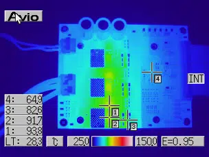
The system remained active until the steady-state condition was reached after about 25 minutes. The ambient temperature detected inside the box at the end of the test was about 28°C. Figure 8 shows the heating transient of the board that was derived from temperature markers and Figure 9 shows the final temperatures on the board.
Figure 8: Measured thermal transient curve – EVALSTDRIVE101 warmup at 15Arms
Figure 9: Thermal measurement – EVALSTDRIVE101 steady-state thermal image
The measurement showed that Q1 MOSFET was the hottest component of the entire board with a temperature of 93.8°C, while the Q4 MOSFET and R23 resistor reached 91.7°C and 82.6°C, respectively.
As discussed in previous section, the Celsius Thermal Solver simulated the Q1 MOSFET temperature at 94.06°C, the Q4 MOSFET temperature at 93.99°C, and the R23 temperature at 85.58°C giving a very good matching with measurements.
Conclusion
STMicroelectronics recently released the EVALSTDRIVE101 evaluation board for use in high power and low voltage three-phase brushless motors for battery powered applications. The board includes a compact power stage of only 50 cm2, which can deliver over 1kW power and 15Arms current to the motor without heatsink or additional cooling.
The use of different simulation features within the Celsius Thermal Solver enabled the designer to not only to predict the temperature profile of the board and its hot spots on power stage components, but also to have a detailed description of voltage drops and current density along power traces, which could be problematic or not feasible at all to obtain by experimental measurements.
Celsius simulation outputs enabled a fast optimization of the PCB layout, placement adjustments, and layout weakness corrections from early in the design to signoff. A thermal characterization with an infrared camera showed good agreement between simulated and measured steady state temperatures, as well as the transient temperature profile, validating outstanding performance of the board and effectiveness of the Celsius Thermal Solver in helping designers to reduce design margin and achieve quick time to market.
References
- L. Coppola, D. Cottet and F. Wildner, “Investigation on current density limits in power printed circuit boards,” 2008 Twenty-Third Annual IEEE Applied Power Electronics Conference and Exposition, 2008, pp. 205-210, doi: 10.1109/APEC.2008.4522723.
- Application Note “Two-Resistor Model for Thermal Simulation” by RHOM Semiconductor.
