Introduction
Reduction in early life failures and continuous quality improvements are “table stakes” for semiconductor manufacturers servicing the automotive industry. “Industry analysts expect that the automotive semiconductor market will be the fastest growing end use market for chips from 2017–21, with a 6.4 percent CAGR and a total market value of between $39-42 billion with conventional vehicles contain an average of $330 value of semiconductor content while hybrid electric vehicles can contain up to $1,000 and 3,500 semiconductors.” [1] The global power electronics market size is projected to grow from USD 35.1 billion in 2020 to USD 44.2 billion by 2025, at a CAGR of 4.7%. [2] To satisfy the automotive quality standards to support this market growth, semiconductor companies are still challenged to achieve zero defects and continue to look for new ways towards this goal.
Historically, semiconductor companies would deploy early life failure reduction efforts with electrical testing or geospatial techniques to reject or test out potential failures. Burn-in and predictive test techniques like part average testing have been around for a long time. Additionally, other geospatial methods, such as visual defect screening and algorithmic yield clustering looking for abnormal patterns, are used to predict early life failures. In the quest for zero defects, companies must reduce defects and also reduce variability. As thermal metrics are one of the most important characteristics of a power electronics component, inline thermal resistance measures add another road to quality for semiconductor companies. Furthermore, the quality of the manufactured components heavily depends on the stability of process parameters which are not always simple to control.
As an example, the materials used in die attach compounds contain chemicals that are hygroscopic in nature. Moisture is absorbed from the environment when the material is exposed. Consequently, any temperature increase during the curing process can result in moisture evaporation that leads to voiding. The die attach pastes also contain volatile compounds which can outgas and cause voids with elevated temperatures. Voids can also arise from the thawing of the die attach paste. The pastes are typically stored in plastic syringes at -40°C. During the thawing process prior to the application of the pastes, there is a difference in the coefficient of thermal expansion between the plastic and paste, which can trap pockets of air at the interface between the two different materials. This can then lead to voids when the paste is applied.
The presence of voids in die attach joints can lead to the development of cracks and interfacial delaminations. If the packages are subjected to a reflow process, any absorbed moisture will vaporize, resulting in higher stress concentrations and the formation of cracks. Interfacial delaminations are caused by voids near or at the interfaces. The presence of these voids reduces the adhesion between the two surfaces, and potentially leading to failure.
Besides the adverse effects on the mechanical strength of the packages, the presence of these defects in the die attach layer will increase the overall thermal resistance of the package, and hence negatively affect the junction temperatures of these devices. The lifetime and reliability will be reduced accordingly.
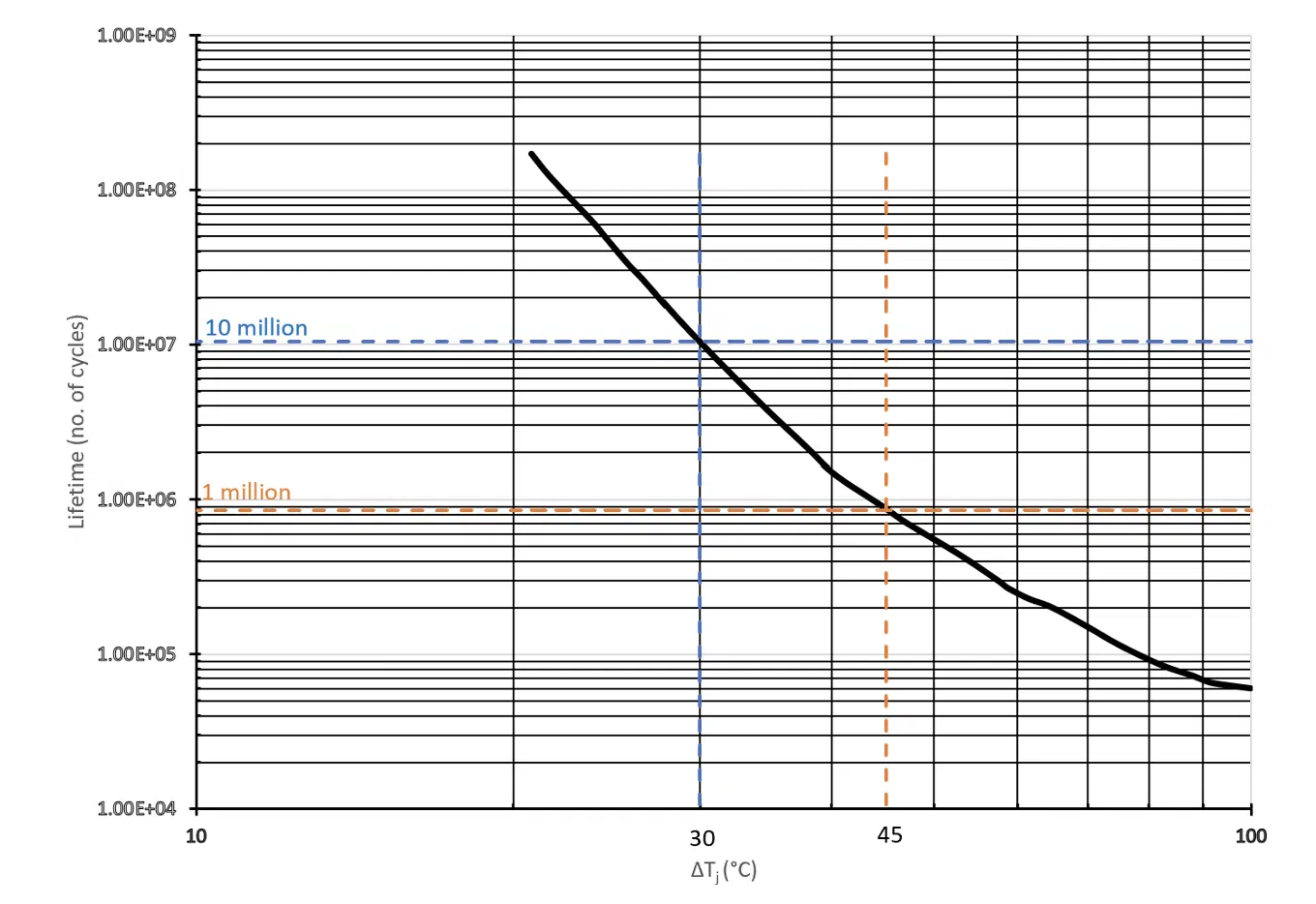
We can quantify this using the power semiconductor example in Figure 1. The lifetime curve for this device operating at the maximum junction temperature is shown. The typical and maximum junction to case thermal resistances of the device vary between 0.14-0.17K/W. Using an average value of 0.15K/W for illustration purposes, a small increase of 5% in the thermal resistance due to the presence of voids, will give a value of 0.1575K/W. This will increase the junction temperature by just under 14°C. The number of cycles to failure is reduced from 26 million down to 1.6 million – corresponding to a tenfold reduction in the expected lifetime of the device.
Figure 1. Thermal resistance variation impact shown on a lifetime curve for a power semiconductor device
Thermal Quality Test Process
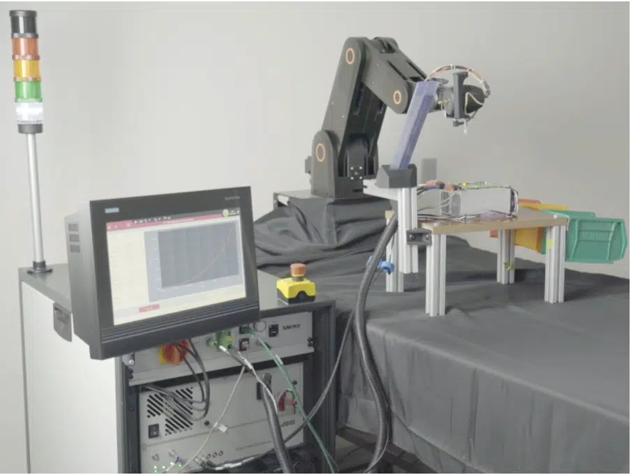
In contrast to the visual identification of die attach voids, transient thermal testing can be used to detect the presence of any defects [3]. The tester communicates with an external handler, a robotic arm in our example, to pick up the components, place them onto the test jig, and bin them after the automatic evaluation is completed. This processes cycles continuously until all samples are evaluated and binned.
Figure 2. Tester with optional robotic arm
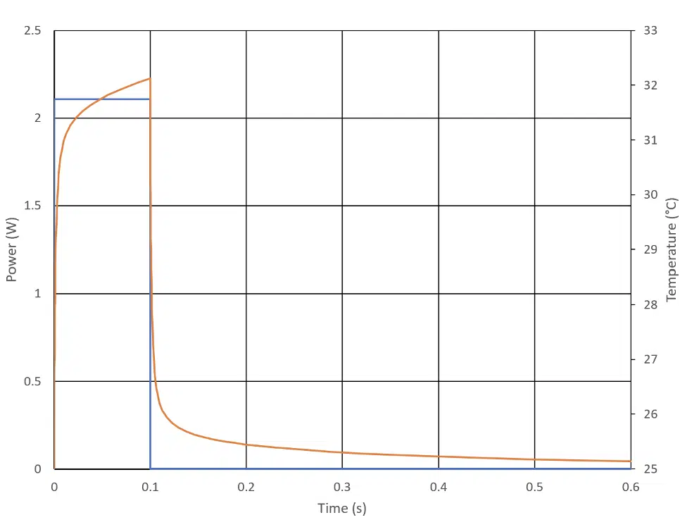
During the actual device test, a short heating pulse is supplied to the die and then turned off. This is followed by a brief cooling period where the temperature data is captured (Figure 3). The heating and cooling times will vary according to the design and internal layout of the packages to be tested, but typically, these will be in the order of maximum a few hundred milliseconds. This is sufficient to detect any defects within the structure. Consequently, the total testing time for a device, including the time for the external handler to position the device onto the test jig and bin it afterwards, would be on the order of seconds, at most. Hence the test throughput for this would be extremely high, and it will be possible to test every single component after the assembly process.
Figure 3. Reduced heating and cooling times for thermal quality tests
In a production environment, it is not necessary to carry out a full thermal characterization test for every single component. A shortened testing time that is able to sense the thermal response of the defective layer will be sufficient. Based on the theory established by Prof. Szekely, the mimimum heating time required to resolve the layer is one order of magnitude longer than its time constant. [4]
A process for implementing and improving thermal quality testing is shown in Figure 4. This involves an initial thermal characterization test of a golden reference device (good sample without any defects). The results from this test is used as the reference for comparisons with the other samples to be tested.
Figure 4. Thermal quality test workflow
Additionally, the structure function curve for the golden reference is used to calibrate a thermal simulation model created using commercially available software [5]. An accurate thermal simulation model is useful for investigating the presence of voids and to quantify how the overall thermal resistance of the packages will change with respect to the void size variation. Ultimately, the results from the void tests can be used to set the binning criteria for the tester.
The thermal quality tests can begin once all the previous steps are completed. The flowchart in Figure 4, includes a fourth step marked in yellow. This represents a potential approach in which the collected test data are used to finetune the binning criteria by overriding the recipe files that define the test conditions.
Initially, the binning criteria is manually set by the operator (Figure 5). Multiple bins can be defined, and the minimum and maximum thermal resistance values are specified at different time intervals. These bands are displayed graphically in the software.
Figure 5. User defined binning criteria. Three bins are created – good (green), medium (yellow), and poor (red)
Devices whose measured thermal resistances fall within the preset, defined bands will be placed in the correct bin automatically by the test handler. The implementation of different bins can improve the production yield by reducing the number of faulty components in assemblies.
Identifying Binning Criteria
Thermal simulations using of a TO-220 device were carried out (Figure 6). The objectives for these tests were to determine the suitable measurement times for this device, quantify the thermal effects of die attach voids and also to use the simulation results to determine the binning criteria.
Figure 6. TO-220 MOSFET structure used in the thermal simulations
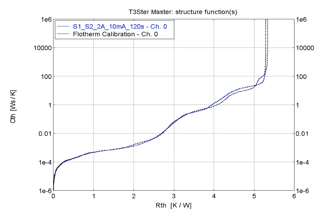
This device was measured previously with a transient thermal tester [6] and the test results were used to calibrate the simulation model prior to any die attach void investigations. Figure 7 shows the results of this automated calibration exercise. With a calibrated thermal model, we would be confident of the accuracy of the thermal and transient response of this device for our subsequent investigations.
Figure 7. Thermal model calibration result
Voids within the die attach layer of the package were then simulated through the use of cuboid blocks, as seen in Figure 8.
Figure 8. Simulated voids emanating from the top left corner of the die attach
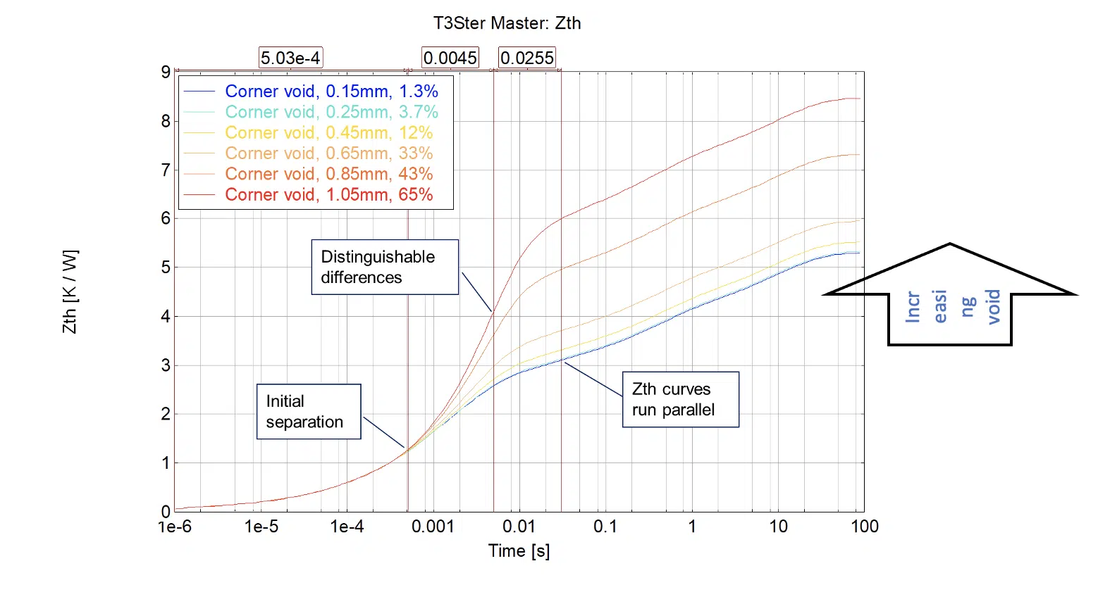
Different void sizes were modelled, ranging from 1.34% to 65.71% by volume and resultant thermal impedance curves are shown in Figure 9. The larger the void size, the higher the temperature elevation.
Figure 9. Thermal Impedance curves of the corner void simulations
Thermal impedance curves are suitable to observe the effects of voids in the model, structure functions can later help to analyze the exact location of the void. The thermal impedance curves can also be used to estimate the required measurement times. In this case, we see that the curves begin to diverge at around 0.5 ms. At 5ms, we are already able to distinguish the differences between most of the cases. By around 30 ms and beyond, the thermal impedance curves become parallel to one another. By delaying the measurement time to 50 ms, we would ensure that heat flow path within the package has travelled to the die attach and beyond. Visually, it is possible to view the differences in thermal resistance or thermal impedance for all the different void size cases. The only two exceptions are the two initial cases with void sizes of 1.34% and 3.72%. The curves for both lie very close to the no defect case. This indicates the lower limit of the detectable void sizes on thermal impedance for this device under test.
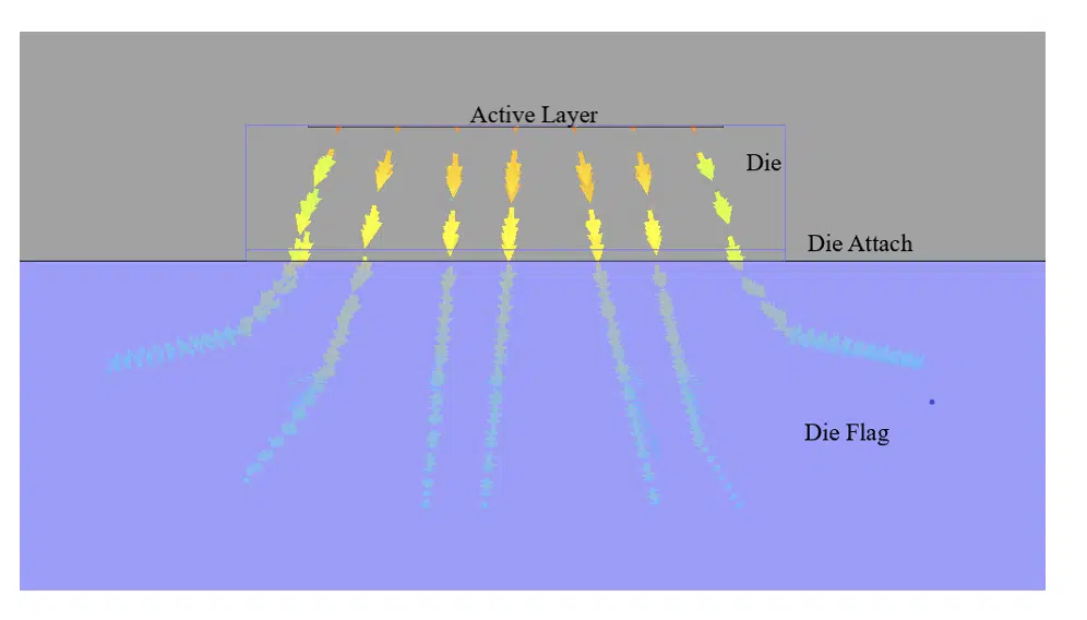
Figure 10. Heat flux vectors developed within the TO-220 package
We are able to visualize the heat flow path within the package by plotting the heat flux vectors developed at 50ms, as shown in Figure 10. The heat travels down towards the heatsink upon which the device is mounted on. It then spreads out in a conical fashion towards the other structural layers within the device.
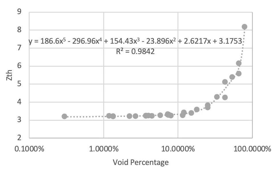
Figure 11. Thermal Impedance and void size relationship for a TO-220, and the binning
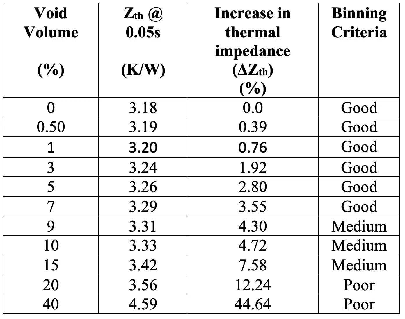
Besides the corner voids, other scenarios with voids in the centre of the die, different numbers of voids and different shapes of the voids, were also considered. These tests, summarized in Figure 12, show an increasing thermal impedance (Zth) values with greater void sizes. A polynomial curve fit can be constructed to quantify this relationship between the two variables. From this relationship, we can calculate the thermal impedance values at a specific time corresponding to the measurements. From there, we use the percentage increase in thermal impedance as the criteria for binning. In this example, any samples with a ∆Zth < 4% will go to the ‘Good’ quality bin. The ‘Medium’ quality bin is 4% < ∆Zth < 15%. Samples with ∆Zth ≥ 15%, will go to the ‘Poor’ quality bin. Table 1 shows examples of this.
Table 1. Binning criteria based on simulation results
In conclusion, a transient thermal tester is capable of quickly detecting the presence of defects within the package thermal structure with non-destructive testing. The method equally works with assemblies, but the required heating and cooling times increase accordingly. All measurements are compared to data collected from a reference sample, in the thermal impedance space. Binning criteria can be easily defined, either based on simulation experiments or real physical tests.
Binning criterion would help define the absolute maximum ratings of the components. Components that would be rejected using stringent yield criteria could now be used for less demanding performance requirements. Binning based on this thermal metric would allow widening of the product portfolios for various applications and markets.
The ability to test every single component in production is a key advantage in power electronics as component manufacturers can reduce infant mortality of their components, track component thermal information and meet increasingly stringent quality and reliability requirements demanded by the current vehicle electrification megatrend.
References
[1]https://www.usitc.gov/publications/332/executive_briefings/ebot_amanda_lawrence_john_verwey_the_automotive_semiconductor_market_pdf.pdf
[2] https://www.marketsandmarkets.com/Market-Reports/power-electronics-market-204729766.html?gclid=Cj0KCQjwvYSEBhDjARIsAJMn0lggEHgHsasGccQXgLPKmlFnJ2p8iQMEDg7Gzifw3PCBuC9eN3BYQOgaAmODEALw_wcB
[3] SimcenterTM MicredTM Thermal Quality Tester – https://www.plm.automation.siemens.com/global/en/products/simcenter/micred-quality-tester.html (last visited on the 28th of May, 2021)
[4] V. Székely, “Evaluation of short pulse and short time thermal transient measurements”, Microelectronics Journal, Volume 41, Issue 9, 2010, Pages 560-565
[5] Simcenter FlothermTM – https://www.plm.automation.siemens.com/global/en/products/simcenter/flotherm.html (last visited on the 28th of May, 2021)
[6] Simcenter Micred T3STER – https://www.plm.automation.siemens.com/global/en/products/simcenter/t3ster.html (last visited on the 28th of May, 2021)
Simcenter, T3STER, and Simcenter Flotherm are trademarks of Siemens Industry Software Inc., or its subsidiaries or affiliates, in the United States and in other countries
