Written by: Dr. Amy Marconnet and Meghavin Bhatasana – Purdue University
Although miniaturization of electronic components has helped advance computing power and accelerated technology development, it has increased power densities and exacerbated the already challenging issue of electronics cooling at the component level. Continuous operation at high temperatures degrades functionality and reduces long-term reliability of electronic devices. As a result, the computational power of these devices is often throttled to prevent such damage. Phase change material (PCM) embedded heat sinks, attached to chips, can increase the thermal capacitance of the system to enable longer periods of operation at full power before throttling or shut-off is required to prevent damage. However, the numerous materials between the heat source and the PCM-laden heat sink limit their effectiveness. Embedding the PCM at the silicon die level, close to the heat source, reduces the resistance pathways associated with chip packaging and traditional bulk PCM-laden heat exchangers. The proximity of the heat source to the PCM (or “thermal capacitor”) allows for the thermal management of transient heat loads and hotspot mitigation. Another important benefit of this embedded PCM strategy is that it provides a compact and passive cooling solution. This is ideal for mobile applications, which require cooling solutions that do not increase the package dimensions. Strategic placement and choice of the PCM (including its melting point and thermophysical properties) also reduce fluctuations in the hotspot temperatures for transient power cycles via the cyclic melting and freezing of the PCM. Here we leverage machine learning tools to enable computationally-efficient optimization of the system performance. Specifically, we evaluate the merits of embedding the PCM directly within the silicon chip through computational modeling and machine learning optimization.
System Configuration
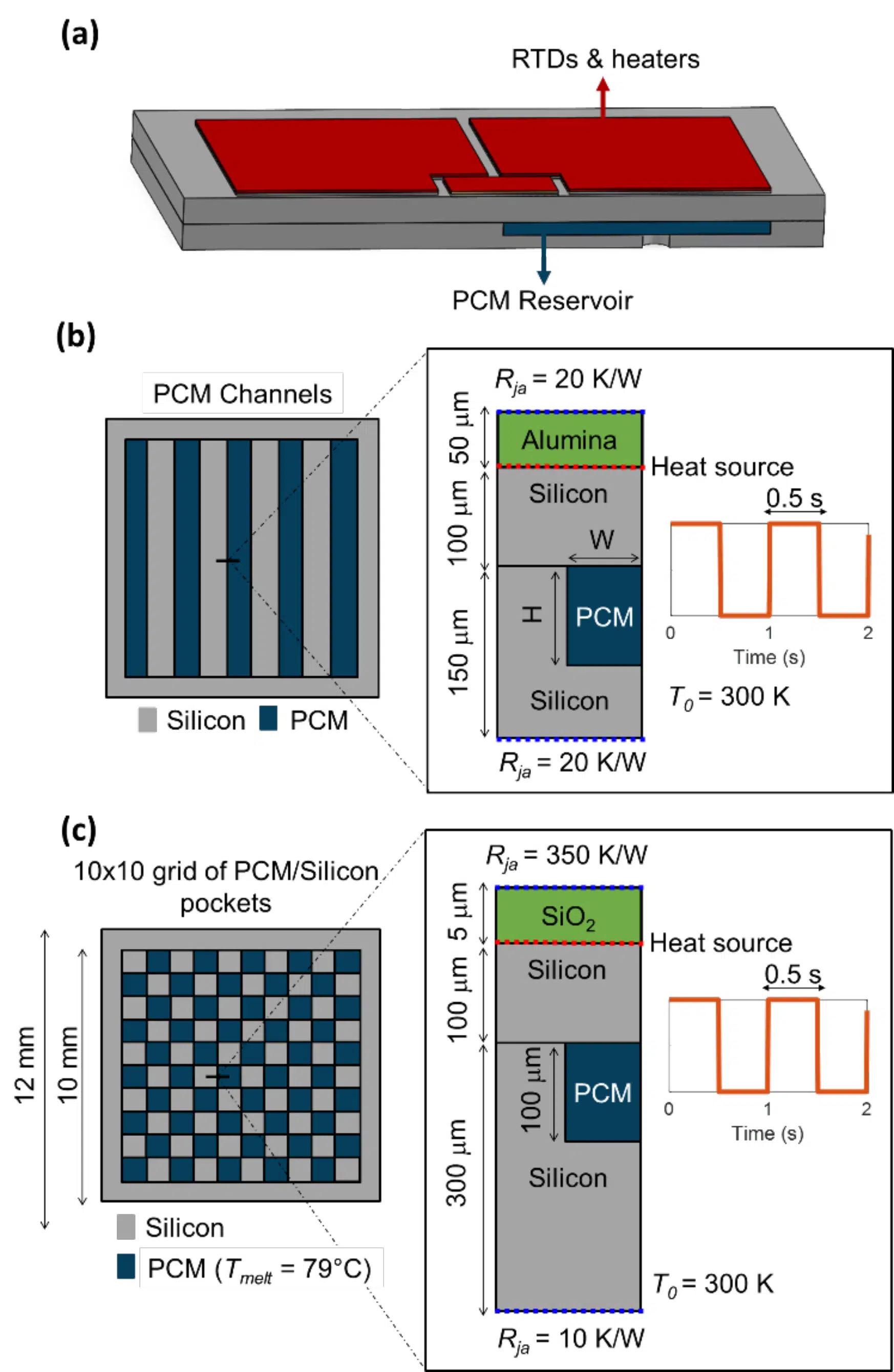
Figure 1 illustrates the silicon-based device of interest. Heaters mimic the power generated in electronic devices and channels or pockets are etched in the silicon to embed the PCM within the silicon device. They are passivated with an oxide or alumina layer. Thermal resistances (Rja) between the external surface of the device are representative of the conduction and convection pathways from these surfaces to ambient. To emulate transient heat fluxes representative of devices in operation, the heat generation is modeled as a periodic square wave with an on/off time of 0.5 s.
Thermal analysis is performed using a MATLAB-based simulation tool developed by the Army Research Lab called ParaPower [1]. It utilizes an implicit Euler finite difference scheme integrated with a 3D thermal resistance network to quickly compute the temperature evolution of the electronics module. ParaPower is noted to be >100 times faster than commercial finite element analysis (FEA) packages while ensuring reasonable accuracy (<2oC) [2].
Figure 1: Overview of the device geometry and thermal conditions including (a) a schematic of the PCM-embedded chip geometry including resistive heaters, the silicon chip, and PCM reservoir and details of the geometries used for (b) 2-D and (c) 3-D optimizations. The key differences are the boundary conditions and the thickness of the sealing silicon layer. The insets in b-c illustrate the cross-section of the chip, as well as the boundary conditions and heat source considered in this study.
Here, two metrics are defined to quantify the effectiveness of the embedded PCM cooling strategy:
To−max: Overall maximum chip temperature (across all time steps)
Tosc: Magnitude of the oscillations in the transient maximum chip temperature Tmax(t) at quasi-steady state
Note that at a particular instant in time, the transient maximum chip temperature is referenced as Tmax, while To-max corresponds to the maximum temperature across all simulated timesteps.
Machine Learning Tools
Machine learning encompasses algorithms and tools that enable computers to learn methods and understand datasets without being explicitly programmed to do so. Machine learning has expansive usage in society. On a daily basis, people interact with machine learning algorithms through Google’s search engine, Netflix’s show suggestions, and automatic chatbots. They are also used extensively behind the scenes in self-driving technology, medical imaging and diagnostics, mail sorting, and stock trading [3].
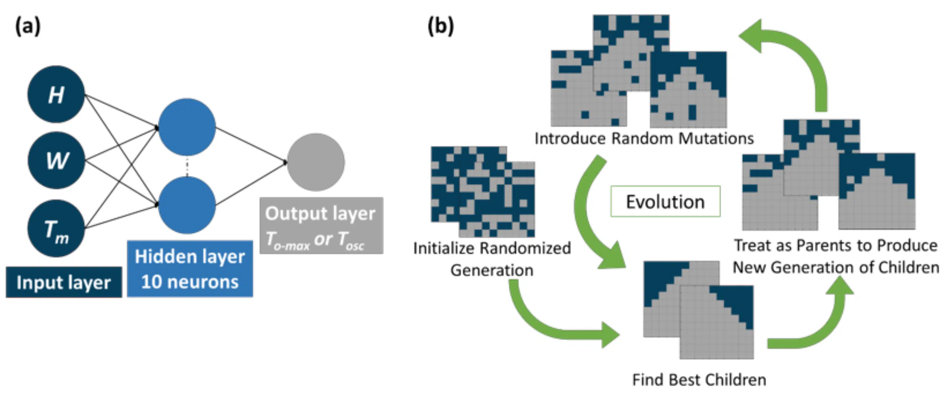
To identify the best configuration of the PCM within the chip, we use a popular evolutionary algorithm, called a genetic algorithm (GA). The GA solves optimization problems based on the concept of natural selection. After generating a randomized population set, it selects the best performing individual solutions and evolves them (by crossing over properties and introducing mutations) cyclically until an optimized solution is found. The optimization algorithm can be coupled directly to ParaPower. We use this approach for both the parallel PCM channels (simplified to a 2D geometry, see Figure 1b) and for the grid-based structure optimization (see Figure 1c). More details about GAs can be found in Ref. [4].
To increase the computational efficiency for the optimization of the parallel PCM channels, we make use of artificial neural networks (ANNs) as surrogate models. Specifically, data from the ParaPower (PP) model is used to train computationally efficient ANNs that are later used for parameter optimization. An accurate ANN enables rapid thermal analysis and, in turn, enables rapid optimization. They are based on the concept of biological neural networks in brains and consist of several processing layers that are interconnected via nodes (called neurons). These layers can be broadly classified into 3 layers: the input layer, the hidden layer(s), and the output layer. The input layer receives information from the user and processes it to the hidden layers, which then process it to the output layer. Any time a layer transmits data to the subsequent layer, it introduces a non-linearity using an ‘activation function’. ANNs are robust and have the potential to accurately model non-linear relationships between independent and dependent variables. For more details on ANNs, we refer the reader to Ref. [5].
Figure 2: (a) Illustration of the ANN architecture used to predict To-max or Tosc. The input layer takes height (H), width (W) and the PCM melt temperature (Tm) as inputs and processes them to the single hidden layer with 10 neurons. Here, a Tan-Sigmoid activation function introduces non-linearity. The data then passes over the output layer to predict either To-max or Tosc. (b) Visual representation of the GA for grid based PCM geometry. When the GA is used with the ANN, the GA cycles between numerical inputs for H, W and Tm.
Embedded Cooling Optimization: Parallel Channels
First, we optimize a 2-D geometry consisting of parallel channels of PCM (see Figure 1b). We explore a multi-parameter optimization of the channel geometry and PCM melt temperature (other thermophysical properties are fixed since they must simply be maximized).
We consider two optimization strategies for this study:
Direct optimization where the genetic algorithm is directly coupled to ParaPower (GA+PP).
ANN assisted optimization where the genetic algorithm is integrated with a neural network (GA+ANN). The ANN is built using training data generated with ParaPower and is validated using a separate dataset of 500 cases. The R2 of the ANN with respect to this testing dataset is reported here. Note that the results shown here for this strategy report the average of ten different runs. Once we generate the data, the ANN is trained ten times with random distributions of the training, validation, and test subsets. Each of these 10 ANNs is then paired to the GA. After the data set generation, the ANN training and GA prediction takes about ~10 seconds.
Comparison Between the ANN and Direct Optimization
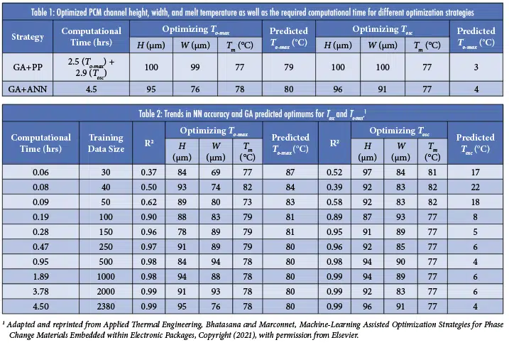
We consider the optimization of the PCM melt temperature and the height and width of the PCM channels. The other PCM properties were fixed to that of Alloy 174, which is a metallic composite that melts at 79°C. A parametric sweep for this study would have taken about 28 days, whereas the machine learning strategies generated effective results within 3 hours. Results of the optimization studies are shown in Table 1.
When optimizing for minimizing the amplitude of the temperature oscillations Tosc, the GA directly integrated with ParaPower (GA+PP) identified filling the entire layer with PCM with a melt temperature of 77°C. The channels occupying the entire available volume may be in part due to the uniform heat source. For minimizing the overall maximum temperature To-max, the strategy predicts the same optimal melt temperatures but leaves a thin silicon channel for conduction.
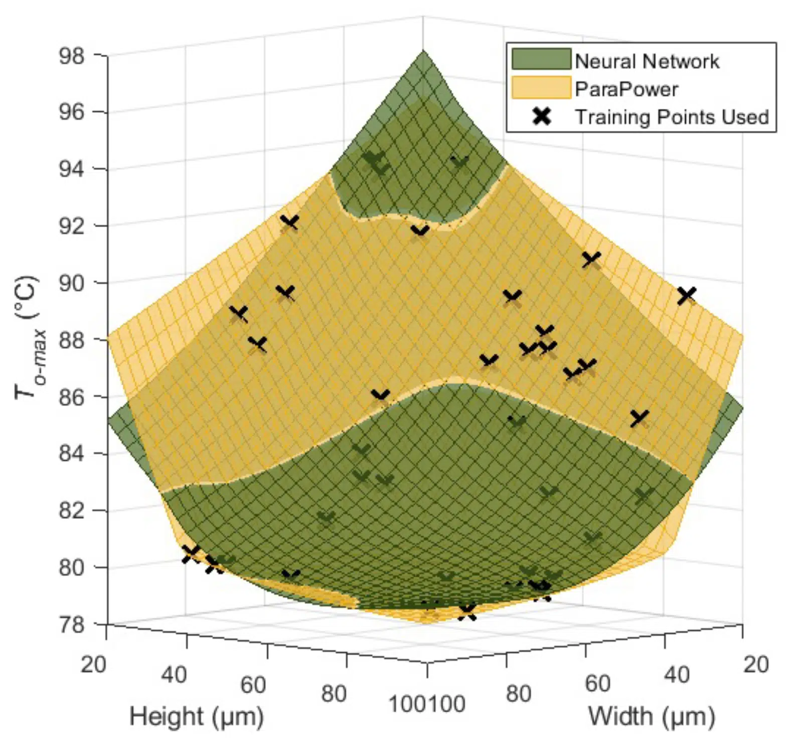
Figure 3: To-max predictions by a NN (shown in yellow) alongside ParaPower predictions (shown in green). The NN prediction have a distinct minimum at a height of 100 µm and width of 75 µm that likely accounts for differences in predicted optima.1
The ANN-assisted strategy predicted a similar trend of having almost filled PCM channels and a melt temperature of 77°C when optimizing Tosc. However, it converged on a melt temperature of 78°C and a channel width that is lower than the upper width boundary for
To-max. This may be due to the ANN inaccuracy near the optimized data range. To explore this, Figure 3 compares the NN model predictions To-max to the ParaPower results over a range of heights and widths with a fixed PCM melt temperature of 78°C (which was the predicted optimal melt temperature for the GA+NN strategy for To-max). However, the ANN predictions do match the general shape of the ParaPower predictions, unlike the continued downward slope of the ParaPower profile, the ANN predicts a distinct minimum To-max near a height of 100 μm and a width of 75 μm. This is why the GA reports an optimum width that is not at the upper bound. The relative flatness of the ParaPower results above a width of 60 μm shows that, despite this unphysical minimum, the impact on system performance is minimal.
Impact of Training Data Set Size on ANN-Assisted Optimization
The results of an ANN-assisted optimization strategy depend heavily on the accuracy of the ANN when compared to the selected optimization algorithm and its set convergence criteria. The performance of an ANN can be impacted by the structure of the ANN (number of hidden layers, number of neurons per layer, activation function, training algorithm), the amount of training data and its subset distribution, and the randomly initialized weights.
Table 2 shows results while varying the size of the training data set for the optimization of To-max. Increasing the training data does not hurt the performance of an ANN, but there are diminishing returns with continuing to increase the training data, with the corresponding increases in computational time. Here, the benefit of increasing the training data stagnates past a data size of 250 cases, with the predicted To-max for the optimized data set for this ANN and the ANN with 2380 cases being only within <1oC of each other. This shows that the parameters for the system optimum can be found within ~30 minutes, which is 13 times faster than the direct optimization coupled to ParaPower.
Embedded Cooling: Grid-Based Geometry
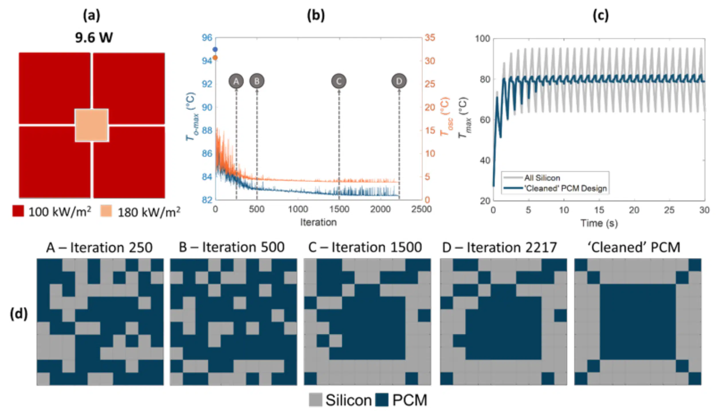
To enable broader optimization of geometries beyond parallel channels with uniform heating, the viable PCM layer is discretized into a 10 x 10 grid of pockets that could be either PCM or Silicon (Figure 1c). The strategic placement of these pockets is optimized through the GA using a binary matrix: 1 denotes a PCM pocket and 0 denotes a silicon pocket. The GA has an optimization objective of minimizing To-max. We chose a metallic composite PCM with a melt temperature of 79oC; based on the results of the 2D parallel channel optimization.
Figure 4: (a) Illustration of the powermap used for 3-D optimization (b) Performance of PCM embedded substrate as GA progress through 2217 iterations. (c) Thermal response of an unaltered all-silicon substrate compared to the optimized substrate. (d) PCM/silicon placements at various points in the GA Progression. The iteration locations are also noted in (b).
A power map (Figure 4a) is defined by first separating the heating layer into 4 large quadrants with a 2×2 cm hotspot zone in the center. The total chip dissipates 9.8 W. The GA optimization takes a total of 2217 iterations to optimize with a total computational time of 25 hours. Figure 4b shows the overall maximum temperature and amplitude of the temperature oscillations at each iteration of the optimization. Figure 4c shows the corresponding temperature evolution for the initial all-silicon starting point compared to the final design. An animation showing the evolution of the design and temperature metrics is available via bit.ly/MTEC_ML1, and for other heating patterns at bit.ly/MTEC_ML2 and bit.ly/MTEC_ML3.
The starting point (iteration 0) of the GA evolution graph (Figure 4b) shows the response for an all-silicon die. The reduction in To-max and Tosc after the very first iteration highlights the substantial improvement in system performance achieved with any addition of PCM. At iteration 250, there is no noticeable pattern in the PCM distribution: the PCM and silicon pockets are randomly distributed. At iteration 500, there are substantially more PCM pockets than silicon pockets. There is a visible pattern by iteration 1500, as the PCM is concentrated in the center as an 8×8 matrix with silicon pockets dominating the outer boundary of the viable PCM layer. The improvement in system performance now stagnates as the GA progress further. The final iterations resemble PCM lines radiating from the middle reservoir of PCM to the corners. A ‘cleaning’ operation is performed on the GA optimized pattern by leveraging symmetry and removing noticeable outliers such as ‘islands’ of PCM that are surrounded by silicon and vice versa. This ‘cleaned’ PCM design reduces To-max by 15% and has the added benefit of reducing Tosc by 80%.
Conclusions
To summarize, machine-learning based optimization with or without surrogate models improves the computational efficiency of the design process for embedded passive cooling layers. With the metallic PCM, adding PCM to the system significantly reduces both the maximum temperature and amplitude of temperature oscillations. These systems are of particular interest for passive cooling of mobile electronic devices and the embedded thermal capacitance can improve system performance. Beyond electronic devices, this same design strategy can be applied to other thermal management applications such as for batteries, automotive, and space applications.
References
[1] ARL ParaPower, https://github.com/USArmyResearchLab/ParaPower
[2] L. Boteler, Multiple Domain Optimized Power Packaging, https://d2vrpothuwvesb.cloudfront.net/uploads/techops/fe1193cf-aa80-4708-b52a-762d2db1c00e/attachments/FY17-OCOH-ScMvr-33-Multiple-Dom_E7PFqYn.pdf
[3] IBM, What is Machine Learning? – https://www.ibm.com/cloud/learn/machine-learning
[4] Mathworks, How the genetic algorithm works. – https://www.mathworks.com/help/gads/how-the-genetic-algorithm-works.html
[5] Mathworks, What Is a Neural Network? – https://www.mathworks.com/discovery/neural-network.html
[6] Bhatasana and Marconnet, “Machine-learning assisted optimization strategies for phase change materials embedded within electronic packages”, Applied Thermal Engineering, Accepted and In Press, 2021. https://doi.org/10.1016/j.applthermaleng.2021.117384

