The creation, transport and storage of digital information are growing at rates of 40% to 50% annually, with video, mobile broadband, and machine-to-machine communication being the main drivers. The implementation of 5G wireless networks is enabling this growth and heralding a new era of revolutionary applications and functionality due to bandwidth increases and communication latency reductions. Key 5G network enablers include new frequency spectrum (e.g., mmWave), massive multiple-input/multiple-output (MIMO) technology and new material systems. Silicon germanium (SiGe) is one material system that offers the potential to develop Radio Frequency Integrated Circuit (RFIC) technology integrating many analog functions into a single integrated circuit, thereby realizing significant reductions in system size, with concomitant cost and power savings.
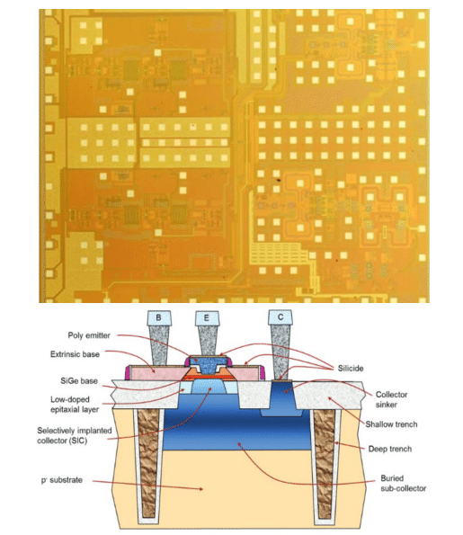
In this article, we present a methodology for simulating die-level heat transfer for an RFIC comprising SiGe devices on a flip-chipped silicon die. This is a challenging thermal problem as the RFIC form factor has shrunk by over two orders of magnitude relative to its analog counterpart, leading to a proportional (100X) increase in heat density that makes package-level thermal management challenging. Fig. 1 shows a photograph of the die studied in this work, which is a transceiver designed for the 27-43.5 GHz frequency range [1]. The goal of the modeling work is to characterize the thermal behavior of the SiGe RFIC to optimize the thermal design and ensure that the device does not exceed the manufacturer-specified Safe Operating Area (SOA) during its lifetime.
THERMAL MODELING
SiGe transistor junction temperature modeling
Fig. 1 (right) shows a schematic cross-section of a SiGe heterojunction bipolar transistor. Modeling the thermal behavior of this transistor using a first-principles, physics-based approach is challenging as it requires precise information about material properties and geometry of the structures comprising the transistor, and which may be considered proprietary and confidential by a foundry.
Figure 1: (top) Die photograph of the 27-43.5 GHz transceiver [1] studied as part of this work; and (bottom) Schematic of a cross section of a SiGe heterojunction bipolar transistor (HBT) [2]
In this work, we utilize an alternative approach based on empirical characterization of individual transistors fabricated by the foundry, where the transistor junction temperature (Tj ) can be represented by the following formula
where Tloc is the local silicon die temperature, Rth,loc(Tloc) is the thermal resistance of the transistor, Pdevice is the transistor power, A and B are empirical constants determined from experimental characterization of the device, and Tref is a reference temperature [3].
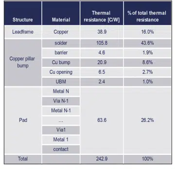
Table 1: Thermal resistance values and relative percentage of the total thermal resistance stack for the leadframe, copper pillar bump and pad as predicted by Eqs. (5) and (6).
Eqs. (1) and (2) provide junction temperature information for low values of Pdevice, where self-heating effects are small. To account for device self-heating, which can result in large local changes in material thermal conductivities, we utilize the model of Paaschens et al. [3], which assumes the device thermal conductivity has the following temperature dependence
resulting in the following equation for Tj
where
kref is the local thermal conductivity of the device at a reference temperature Tref , α characterizes the decrease of the device thermal conductivity with temperature, and Rth,loc (Tloc) is given by Eq. (2).
SOLDER BUMP, CONTACT PAD AND LEADFRAME THERMAL RESISTANCE
The flip-chipped silicon die studied in this work is attached to the leadframe using copper pillar bumps [4][5]. In addition to providing signal and ground connections, the copper pillar bumps are the primary path for transferring the dissipated power from the SiGe transistors. In particular, the layout includes a dedicated subset of “thermal” bumps whose role is for heat transport.
The simplest approach to modeling the layers within the copper pillar bump, pad and leadframe is as thermal resistances in series, e.g.,
where hi , Ai , and ki are the thickness, area, and thermal conductivity of the individual layers. The series resistance approach predicts a total thermal resistance from the pad to the lead frame of 242.9 C/W, with the individual contributions to the total thermal resistance being 26.2%, 57.8% and 16.0%, respectively, for the pad, copper pillar bump and leadframe (see Table 1).
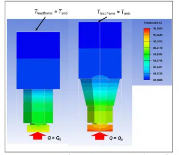
To account for spreading and constriction resistance effects not captured in the series resistance approach, a detailed numerical model was constructed with commercially available software [6]. The computed temperature field is shown in Fig. 2 (next page). This structure has a thermal resistance of
which is approximately 15% larger than the analytical formula, indicating that the analytical series resistance approach is reasonable while the detailed numerical model provides additional accuracy. We also note that the numerical model can be readily extended to account for important effects such as solder wetting; see, for example, Fig. 2 (next page).
Figure 2: Temperature contours for structures comprising a contact pad, copper pillar bump and leadframe: (left) untapered solder region with Rnumerical leadframe+bump+pad = 280 C/W; and (right) tapered solder region with Rnumerical leadframe+bump+pad = 343 C/W.
DIE LEVEL THERMAL MODELING
Approximation to the detailed thermal bump model
The thermal bump numerical model comes at a computational cost, as the grid used to resolve the temperature field can comprise over 1 million nodes. A coarser grid may decrease the computational cost. However, as the application has several hundred thermal bumps, it is anticipated this approach would not scale well computationally. Instead, we replace the detailed model with an approximate boundary condition where the pad interfaces with the silicon substrate

where the left hand side term corresponds to the silicon conductive heat flux, R bump = Rnumerical leadframe+bump+pad is the thermal resistance of the thermal bump as calculated from the detailed computational model, and Apad is the pad area in contact with the silicon substrate.
Fig. 3 shows a comparison of the detailed and approximate boundary condition models. The similar silicon die temperature contours indicate the approximate boundary condition is a reasonable proxy for the detailed numerical model, while the grid size decreased from ~610k nodes in the detailed model to ~91k nodes in the approximate model – a significant computational cost reduction. Simulations show that, for a range of bump to heat source distances, the relative error in the heat source to leadframe thermal resistance is below 2.5%, which is an acceptable tradeoff to realize a computationally tractable die-level thermal model, which we discuss in the following section.
Die level thermal modeling – spread heat source approach
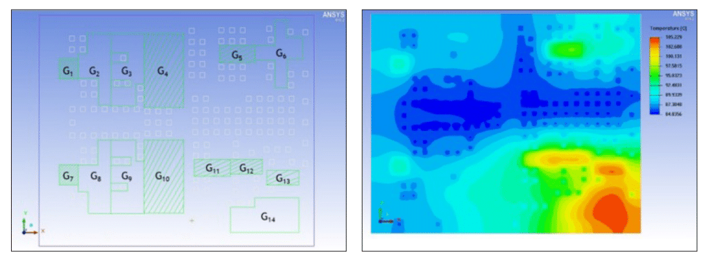
A spread heat source model is constructed by dividing the transistors and supporting devices into 14 groupings, with each grouping Gi assumed to dissipate its power uniformly over the area occupied by that functional block. Fig. 4 (next page) shows the silicon die with the 14 transistor groupings, denoted by the green polygons, with a total heat dissipation of 4.65 Watts. Heat transfer to the lead frame is facilitated by 150+ thermal bumps, denoted by the white squares, while conduction through underfill is accounted for on the remainder of the die.
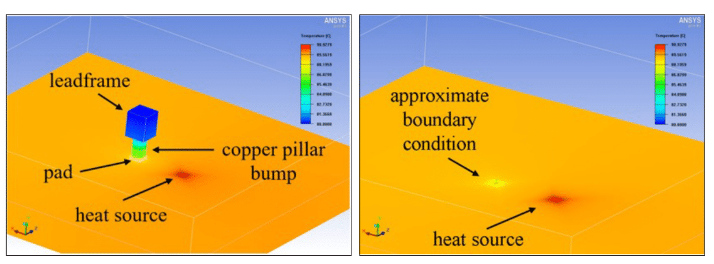
Figure 3: Computed temperature contours for numerical models for detailed (left) and approximate (right) thermal models for heat transfer through a thermal bump (pad+copper pillar bump) that is shifted 300 µm laterally from a 73µm x 73µm heat source dissipating 20 mW on a 200 µm thick silicon die. (color contour range: 80-90.9°C)
Figure 4: (left) Die level spread heat source thermal model consisting of 14 transistor groupings (green polygons) dissipating a total of 4.65 W and 150+ thermal bumps (white squares). The silicon die (purple rectangle) is approximately 4.1 mm (width) x 3.5 mm (height) x 0.2 mm (thickness); and (right) Temperature contours for the spread heat source thermal model presented in Fig. 4 (left). The maximum temperature rise of the silicon die is approximately 25.2°C above the lead frame temperature of 80°C. (color range : 84.8 – 105.2°C)
Figure 5: Temperature contours for the spread heat source model presented in Fig. 4 and incorporating a detailed model for transistor grouping G13. (color contour range: 83.7 – 124.6°C)
Temperature contours across the silicon die are shown in Fig. 4 (above) for the spread heat source model. The maximum die temperature rise is 25.2°C and occurs in the lower right-hand portion of the device. We note that this region contains 47% of the total heat dissipation (from transistor groupings G11 through G14) and has a lower thermal bump density compared to the remainder of the silicon die. The silicon die temperature provides useful information for device designers, for example, to mitigate potential deleterious effects of electromigration, which are accelerated at elevated temperatures.
Most stressed SiGe transistor junction temperature estimation
The results shown in Fig. 4, coupled with knowledge of transistor power densities, indicate that the most stressed transistor is associated with grouping G13, a power amplifier comprising 2 subgroupings of 4 identical transistors. A more representative model of grouping Q13 is constructed by assuming individual transistor power is dissipated uniformly within its footprint and incorporating confinement effects associated with the silicon dioxide/polysilicon deep trench surrounding each transistor. Fig. 5 shows temperature contours for this detailed thermal model of transistor grouping G13, with the remaining transistors groupings modeled using the spread heat source approach. We note that the silicon die maximum temperature is now significantly greater with the localization of transistor heat dissipation in grouping G13; contrast Tmax of ~124.6°C in Fig. 5 with Tmax of ~105.2°C in Fig. 4. The temperature contours shown in Fig. 5 also indicate that transistor PA1 has the highest temperature of the 8 transistors within the grouping G13.
Estimating the junction temperature for transistor PA1 using Eqs. (3) and (4) requires knowledge of the local silicon temperature near this device, namely Tloc,PA1, when this transistor is in the “off ” state. This is calculated by assuming the following power distribution in grouping G13
Tloc,PA1 is plotted as a function of the normalized transistor power Pconst/Pmax in Fig. 6 (next page), where Pmax is the maximum anticipated transistor power.
Knowledge of the local silicon temperature for transistor PA1 allows an estimation of its junction temperature using Eqs. (3) and (4). Fig. 6 (next page) shows the predicted junction temperature for transistor PA1 as a function of the normalized transistor power and for various values of α. We note that the predicted junction temperature at Pconst = Pmax (see inset table in Fig. 6 next page) ranges from 152.4°C for no temperature dependence (α = 0) to 157.9°C for α = 1.333, which is characteristic of bulk silicon, to 161.2°C for α = 2, which is characteristic of foundry data. The predicted junction temperature provides useful information to assess the reliability of the device given potential usage scenarios and to ensure the device does not exceed the manufacturer-specified Safe Operating Area (SOA) during its lifetime.
In summary, this article has presented a modeling approach to characterize the thermal behavior of a SiGe RFIC for wireless communications. Key takeaways and lessons learned from this work include:
• 1D analytical models are useful for initial estimates of copper pillar bump and underfill thermal resistance.
• Detailed computational models are essential for quantifying spreading and constriction resistance effects at the thermal bump, silicon die and transistor footprint levels as well as quantifying thermal cross-talk between adjacent devices such as transistor groupings and individual transistors within a grouping.
• The compact model for heat transfer through the thermal bump is essential for reducing the computational complexity of the overall die-level thermal model with a minimal impact on accuracy.
• Incorporation of empirical foundry data for individual transistor thermal performance into the overall modeling framework allows for realistic estimates of device junction temperatures and obviates the need to construct a first-principles, physics-based model of a SiGe heterojunction bipolar transistor.
Figure 6: (left) Temperature of silicon local to transistor PA1 as a function of transistor power Pconst, with PPA1 = 0, P PA2 = P PA3 = … = P PA8 = Pconst. Note temperature contours local to transistor PA1 shown in the inset image; and (right) Predicted junction temperature for transistor PA1 as a function of transistor power, as predicted by Eqs. (3) and (4) with various values of α.
ACKNOWLEDGEMENTS
The author would like to acknowledge the excellent collaboration and many useful discussions with Joe Weiner, Yves Baeyens, Pascal Boutet, Pierre Lopez and Shahriar Shahramian.
REFERENCES
[1] Y. Baeyens et al., “A Wideband SiGe BiCMOS Transceiver Chipset for High-performance Microwave Links in the 5.6-43.5 GHz Range,” in IEEE Radio Freq. Int. Circ. Symp. (RFIC), 2017.
[2] H. Rucker and B. Heinemann, “SiGe HBT Technology”, in Silicon-Germanium Heterojunction Bipolar Transistors for mm-Wave Systems: Technology, Modeling, and Circuit Applications (pp. 11- 45). N. Rinaldi and M. Schröter, Editors, River Publishers, 2018.
[3] J. C. J. Paasschens et al., “Dependence of thermal resistance on ambient and actual temperature,” in Proc. Bipolar/ BiCMOS Circuits Technol. Meeting, Sep. 12–14, 2004, pp. 108–111
[4] P. Sun et al., “Flip chip CSP assembly with Cu pillar bump and molded underfill”, In 2016 17th International Conference on Electronic Packaging Technology (ICEPT) (pp. 807-811). IEEE, August 2016.
[5] T. Stander, “A comparison of basic 94 GHz planar transmission line resonators in commercial BiCMOS back-end-of-line processes,” in 2014 International Conference on Actual Problems of Electron Devices Engineering (APEDE), vol. 1, pp. 185–192, 2014.
[6] https://www.ansys.com/products/electronics/ansys-icepak
