KEYWORDS
Thermal Resistance | Thermal Interface | Semiconductor Test | Durability | Cycling | Device Under Test
NOMENCLATURE
DUT Device Under Test
OSAT Out-Sourced Assembly and Test
Rth Thermal Resistance
S/TB Semiconductor Test and Burn-In
TIM Thermal Interface Material
ABSTRACT
Many thousands of thermal interface materials (TIMs) exist due to the very wide disparity in requirements across an extremely diverse range of market applications throughout the electronics industry. For certain market segments, such as geothermal and downhole petroleum exploration and semiconductor test and burn-in, application requirements may be so significantly challenging as to require development of materials for very specific and unusual requirements, beyond normal computing equipment and power electronic systems requirements. A test program in four phases has been designed to test such newly-developed materials against those very narrowly-defined and unusual requirements. The value of discussing such materials intended for a relatively narrow market segment is that this type of testing and development work can be useful in evaluating how to develop unusual test programs for other material applications. Three newly-developed TIMs designed specifically to address semiconductor test and burn-in (S/TB) requirements were tested and successfully passed each test phase.
SEMICONDUCTOR TEST REQUIREMENTS
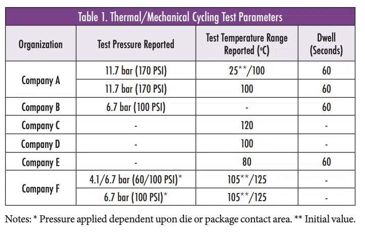
The semiconductor test industry consists of manufacturers of very specialized test systems, companies that develop relatively complex test heads and sockets configured for specialized IC and power semiconductor packages, and the OSATs and semiconductor manufacturers that must perform testing of every device or according to a sampling regimen. This array of different customers for the TIMs utilized all have differing requirements that must be addressed. A short survey of a limited number of these manufacturers was conducted to develop a test regimen for clamping force, contact duration (dwell), temperature, and what is termed a “strike angle” for a non-parallel contact. Test procedures also include operation over a range of temperatures (typically 115-125°C) for defined periods, and, in certain burn-in tests, temperatures to 155°C. Mechanical test characteristics combined together (zero residue on the DUT, non-parallel contacting surfaces and potential for a strike angle as described, elevated temperatures, thousands of contacts with a single TIM) and this set of requirements is a major challenge for durability for any type of TIM selected.
Semiconductor test parameters include a variety of electrical performance tests for device performance and binning by frequency and other characteristics. Elevated temperatures during burn-in testing are intended to stress and cull early failures. The development of a single TIM type that can withstand many hundreds and thousands of contact cycles is critically important to test throughput and cost of semiconductor test. Some highly specialized devices may be very low unit volume, with only hundreds tested per day, while high-volume manufacturers of microprocessors and ASICs may require testing at rates up to tens of thousands per day. Stopping test programs in order to remove the TIM, clean the test head, and apply a replacement TIM can therefore be exceptionally costly in labor time and in yield.
Many different test head designs exist, to meet differing system requirements. Test is divided into two principal design categories: the use of a monolithic test head (i.e., a unitary flat contact surface facing the DUT), and the use of multiple electrical contact pin probes in an array (where no TIM is used). This discussion deals with the majority design category, the monolithic test head. These test head designs incorporate heating and cooling capabilities within the test head, with complex systems utilizing a liquid cold plate, one or more thermoelectric modules, and heaters, to apply the desired temperature cycles. The TIM must be applied to the flat test head surface facing the DUT
MATERIALS DEVELOPMENT FOR SEMICONDUCTOR TEST
The critical requirement for semiconductor test, regardless of material type, is that any TIM used in contact with a device under test (DUT) must be of a type that does not leave any residue, oil, or contaminant on the surface of the device package (or die surface, if a bare die package). This requirement cannot be waived and eliminates all materials that are polymeric, in pad form, and capable of marking or leaving any detritus (especially electrically conductive), and all compounds such as greases and gels. While semiconductor test and burn-in (S/TB) may be a relatively low unit volume market segment, making this market a lesser choice for focusing new materials development, finding a material that will survive one to ten thousand contacts with a single TIM placement is highly desirable for test throughput and cost.
Development of three new materials for S/TB has therefore focused on metallic and graphitic sheet materials. Graphitic materials are difficult to adapt to sharp corners and edges of test heads and also have a potential for shedding electrically-conductive flakes and fibers. Metal TIMs also, depending on metal and alloy selected, may be relatively brittle and have potential for shredding when the test head repeatedly contacts at an angle, on a 90-degree edge or on the sharp edge of a bare die. Taken together, these requirements as outlined in Table 1 are a significant challenge for new materials development.
RELIABILITY TEST PROGRAM DEVELOPMENT
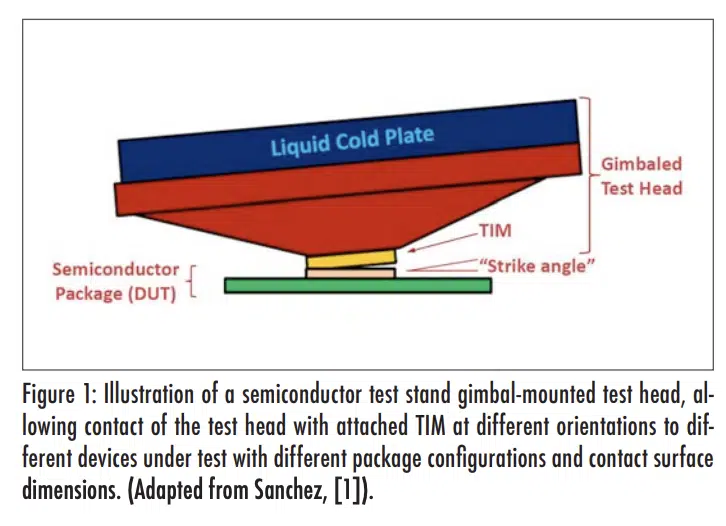
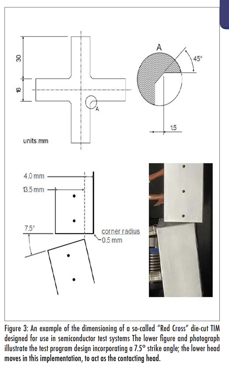
Use of a commercial TIM test stand was considered as the primary tool for a reliability test program. The ability to combine repeated, controlled cycling of a test material (for contact at a specific temperature, dwell, and release), with automated data collection per an industry-standard thermal resistance test procedure, was seen as a constructive approach, given the previously demonstrated reliability testing completed by the test stand manufacturer for other types of thermal materials. The test stand, designed and manufactured by a commercial manufacturer [1] to follow ASTM D 5470-17, incorporates servo motors with precise control of test head movement; a goniometer for planarity measurement; and internal software and motor controls. In addition, test heads are designed to be removable and in the standard system could be adapted to create a non-flat condition, with one test head capable of contacting the second at a pre-determined angle. [2, 3] This latter capability would mimic the so-called strike angle, found in high through-put semiconductor test systems where multiple types of devices (with lid; different lid sizes, different package types; bare die, and similar) flow through the test system. More complex system test heads include a gimbal, to allow the test head surface to adapt to these differences, as shown in Figure 1. [4]
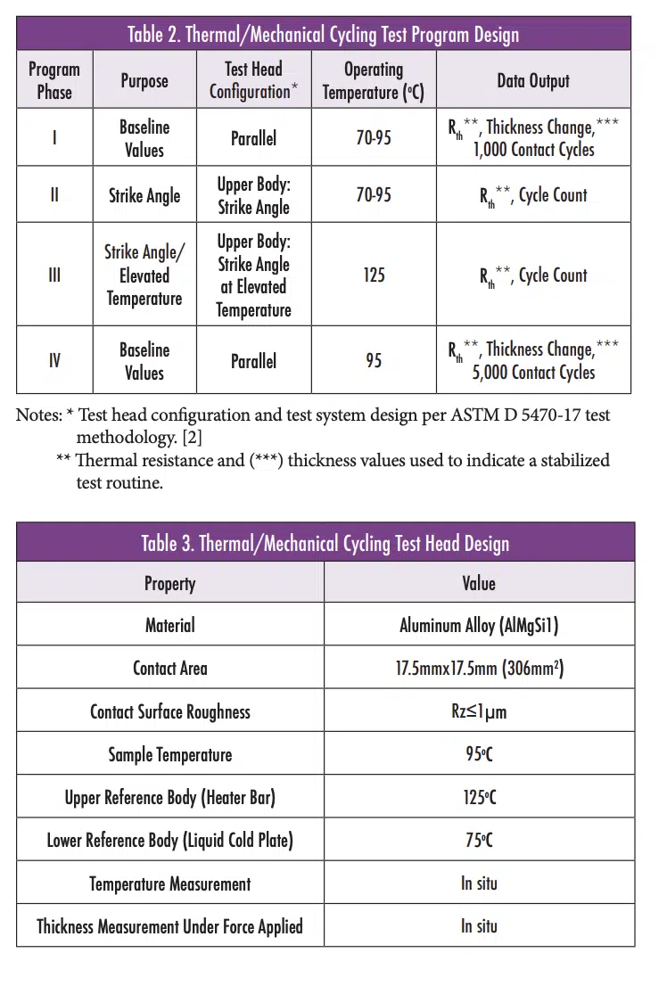
For this test program, four test phases were developed to place increasingly challenging durability requirements on each new development material; simultaneously, TIM thickness change was measured during each phase, as was thermal resistance. The four phases are summarized in Table 2; the first is the baseline set of data against which subsequent data sets were to be compared. Phases I and IV are similar to the conditions required for standard ASTM D 5470-17 thermal resistance testing, with parallel test heads and a uniform power and clamping force applied. [5, 6] Phases II and III address the elevated temperature and so-called “strike angle” introduced to mimic behavior in S/TB processes; the specific characteristics of these two phases were developed from the data obtained in a short industry survey of practice. Phases II and II therefore are not representative of a normal thermal resistance test per industry standard ASTM D 5470-17. (A dwell as short as sixty seconds would normally be considered to be insufficient for system stabilization and accurate data generation.) Specifications for the test heads are shown in Table 3.
MATERIALS TESTED
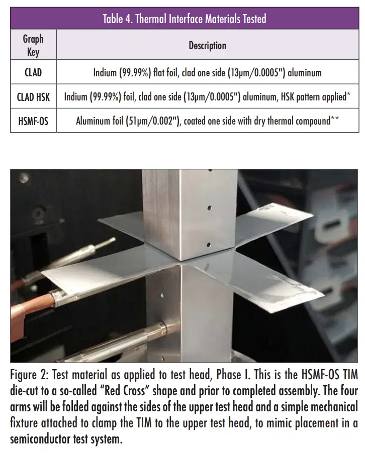
Three recently-developed TIM types were tested. Each of these has been developed to meet specific requirements for semiconductor test and burn-in applications. These are described in brief terms in Table 4; each is a metal alloy. The first is a dead-soft aluminum alloy coated with a non-silicone thermal compound applied to one side only, identified as HSMF-OS. The second and third are indium metal, a relatively compliant metal that can also be moderately tacky. Given the requirement for ST/B applications that the TIM separate cleanly with no residue be left on the DUT, one indium TIM is manufactured with a very thin aluminum alloy cladding; this thin cladding is slightly stiffer and provides the clean separation and more durable surface required. This TIM was originally developed for rework requirements for high-dollar-value semiconductor processor modules for enterprise servers. The first aluminum-clad indium TIM is a flat foil. The second aluminum-clad indium TIM is manufactured with the same construction as the first, with a distinctive patterning applied to increase compliancy. [6]
Figure 2 illustrates one of these specialized TIMs, die-cut to a socalled “Red Cross” shape, as applied to the upper test stand test head. RTDs are evident in the figure, requiring through-holes in the arms of the TIM pre-form, where the RTDs are inserted into the test head after placement of the TIM.
TEST RESULTS AND EVALUATION
The usefulness of the selected commercial test stand [7] was shown in the consistent data, generated without any modification of the system controls and hardware. Automated data output for material thickness change during test was determined to be a useful indicator of any perturbations, whether in electrical power or in material durability. A perturbation was observed in one test due to an input electrical problem, which was corrected. The relatively smooth curve representing measured thickness change proved to be a useful determinant of stable test conditions, with no TIM degradation such as tearing or perforation (with the introduced strike angle). Nominal thermal resistance data was also used as a check for stability during the test regimen, for control purposes. The test system provided output values that included test head temperature measurement, material thickness, changes in thickness (for the selected TIM under test), bulk and interfacial thermal resistance values, and derived thermal resistance (Rth). Designed to incorporate removable test heads, the test program could therefore be designed with specification of contact surface roughness; the use of a fine adjustment feature allowed specification of a precise angle per the “strike angle” for Phases II and III. Such built-in features avoided the need for specially-designed equipment that would have added a cost and time penalty for the program.
Materials subjected to each test phase were examined visually for evidence of cracking, tearing, or other perturbation.
All materials tested exceeded the goal of one thousand contact and release cycles.
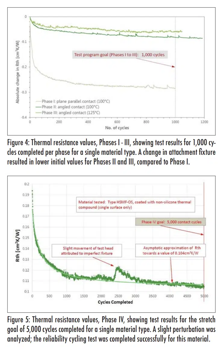
Thermal resistance values for the first three phases of the test program are shown in Figure 4, for one of the development materials. During the cycling regimen, a plot was generated showing thickness change for each material, for each phase; each such graph showed a stable condition. No marking and no residue was found on the test head surfaces, upon completion of each test phase for each material.
Given successful completion of the first three test phases, an additional phase to test to achieve 5,000 contact cycles was conducted. The HSMF-OS material was selected and tested and this stretch goal for the test program was achieved. Again, no evidence of cracking or shredding of the TIM being tested, as well as no evidence of marking or residue left behind. [8]
CONCLUSIONS
This test program was based on a survey of challenging industry requirements for semiconductor test and burn-in applications. Based on the survey, a test program was developed in order to test and evaluate a set of specialized TIMs developed to meet these requirements. The test program consisted of four phases and all three development materials met the goals of these four test phases. The results have been analyzed, with no visible evidence of tearing, shearing, or marking of the devices under test. The indication is that this test program was completed successfully for all three TIM types examined, using a commercially-available test stand designed to follow an industry-standard thermal resistance test methodology. The result of this testing will be used to demonstrate how these specially-designed TIMs can be utilized for these intended applications.
ACKNOWLEDGMENTS
All testing was conducted in an independent test laboratory, Berliner Nanotest und Design GmbH, in Berlin, utilizing a test stand developed by Berliner Nanotest. Industry inputs by Jaime Sanchez, Intel Corporation, and other participants in the industry requirements survey, were very important for practical test program design.
REFERENCES
[1] Berliner Nanotest und Design GmbH.
[2] ASTM International, ASTM D 5470-17, Standard test method for thermal transmission properties of thin thermally conductive solid electrical insulation materials, ASTM International (Philadelphia PA USA, 2017).
[3] Berliner Nanotest und Design GmbH, “TIMA 5 Thermal Interface Material Analyzer Data Sheet,” August 2018, www. nanotest.eu/tima5.
[4] Sanchez, J.A., Intel Corporation, “Challenges of Thermal Interface Materials in Test of IC Packages,” IMAPS Advanced Technology Workshop on Thermal Management 2013, Los Gatos CA USA, November 5-7, 2013.
[5] Lasance, C., Murray, C.T., Saums, D.L., Rencz, M., “Challenges in Thermal Interface Material Testing,” Proceedings, SemiTherm Symposium 23, Dallas TX USA, March 2006.
[6] Jarett, R.N., et al., “Comparison of Test Methods for High Performance Thermal Interface Materials,” Proceedings, Semi-Therm Symposium 23, San Jose CA USA, March 2007.
[7] Nanotest TIMA5 test stand
[8] Saums, D., Jensen, T., “Development, Testing, and Application of Metallic TIMs for Harsh Environments and Non-Flat Surfaces,” Proceedings, IEEE I-Therm Conference 2017, Orlando FL USA, May 30-June 2, 2017.
