Overview
Thermal Design Power (TDP) is a term commonly used in the thermal management of consumer electronics. While the usage of this terminology may vary across the industry, it commonly refers to the amount of power that a device may dissipate indefinitely, in a given thermal environment, without exceeding the temperature limits of the device. The TDP for a consumer electronics device is of great interest because it provides physical bounds to the experience a product can deliver to the user (e.g., phone call, internet, photo capture, gaming, etc.).
Thermal design engineers often have the most influence on a product’s design during its architecture development. It is not uncommon for designs to rapidly evolve in this phase of the design cycle, with real-time changes occurring daily or even hourly. It is also not uncommon for teams to rapidly pivot between multiple concepts. Some first-order tools are essential to provide effective thermal design guidance in a fast-paced environment. Detailed finite element or computational fluid dynamics simulations are often not practical due to the timeline and lack of design maturity. TDP provides one simple and useful metric that can guide the design in the desired direction.
Where We Left Off
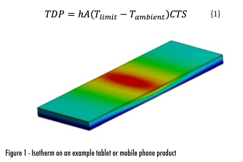
A physics-based method for determining the thermal design power of a passively cooled consumer electronics tablet with in-plane thermal gradients was provided in Part 1 of this column [3]. The thermal design power of a device like that shown in Figure 1 can be calculated using Equation 1, where h is the effective heat transfer coefficient, A is the external area of the device, Tlimit is the touch temperature limit, Tambient is the ambient operating temperature, and the CTS is the coefficient of thermal spreading [1].
When in-plane thermal gradients dominate and the temperature on the front and back surfaces of the device are identical, the CTS can be quantified using the fin equation.
Through-Plane Thermal Gradients
Additional thermal design tools are needed to account for through- plane thermal gradients that develop across the thickness of the device. Even when there are minimal in-plane thermal gradients, a CTS correction to the theoretical thermal design power is required when the front and back surfaces of the device are at different temperatures.
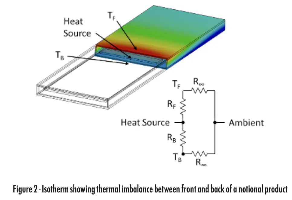
The thermal design power is determined when any point on the surface of the device reaches the temperature limit. Thus, if one side of the device reaches the temperature limit before the other, the device’s ability to reject heat to the environment is reduced. Figure 2 provides a cross-section of a device with different temperatures on its front and back surfaces.
Approach for Calculating CTS with Through-Plane Thermal Gradients
The primary heat source in many consumer electronics products is an electronic component, such as a processor, that is centrally located in the product and mounted on a printed circuit board assembly (PCBA). The thermal architecture of the product defines the heat paths between this heat source and the front and back surfaces of the product, which reject heat to the environment.
One method to evaluate the coefficient of thermal spreading with through-plane thermal gradients is to calculate the thermal resistance values from the heat source to the front (RF) and back (RB) surfaces of the device respectively. The reader is referred to a heat transfer text, such as Reference [2], for details on calculating equivalent resistances through composite structures. For example, the resistance from the heat source to the front of the device may include transfer through a thermal interface material, into a chassis, and then to the surface of the device.
Once the resistances to the front and back surfaces of the product are calculated, the parallel thermal resistance network illustrated in Figure 2 can be used to determine the temperature difference across the thickness of the device, as well as the heat rejected to each surface. The multiplier (Mthrough-plane), defined in Equation 2, falls out of the parallel resistor network, where RF is the resistance to the front surface of the product, RB is the resistance to the back surface of the product, and R∞ is the thermal resistance between the device surfaces and the external environment.
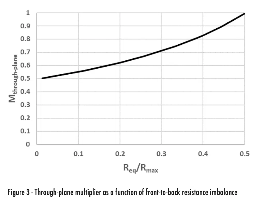
This multiplier quantifies the reduction in thermal design power attributed to through-plane thermal gradients. Figure 3 illustrates this multiplier as a function of the non-dimensional resistance ratio Req/Rmax. Req is defined by Equation 3 and represents the total equivalent thermal resistance from the heat source to the environment (including both front and back surfaces). Rmax is defined by Equation 4 and represents the larger of the thermal resistances between the heat source and the environment (through either the front or back surfaces individually).
When the front and back thermal resistances are equal (Req/Rmax = 0.5), the multiplier equals 1 and the theoretical maximum thermal design power is achieved. When the thermal resistance to one surface of the device is much greater than to the other, the multiplier approaches 0.5, and essentially only one surface of the device is used for heat rejection. The magnitude of multiplier variation illustrates the importance of through-plane thermal gradients in the product design process.
When a product with negligible in-plane thermal gradients exhibits a temperature difference between its front and back surfaces, the CTS becomes equivalent to the through-plane multiplier in Equation 5.
Putting it into Practice
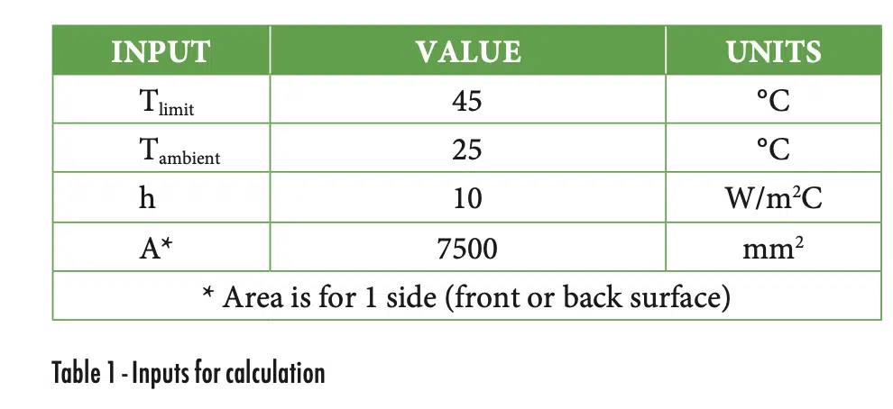
Now let’s demonstrate this for the calculation on a notional device with the inputs specified in Table 1 and negligible in-plane thermal gradients. It is common for the environment, temperature limits, and form factor to be known early in the design process.
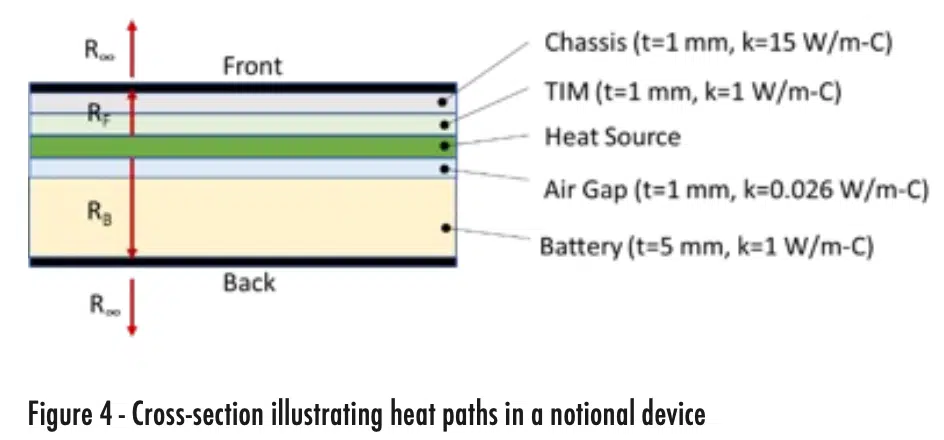
A cross-section of the notional device is provided in Figure 4. Heat is assumed to be generated on a PCB in the middle of the device. Heat leaving the front surface of the device passes through a thermal interface material (TIM) and a chassis. Heat leaving the back of the device passes through an air gap and the device battery. The thickness (t) and thermal conductivity (k) of each layer is specified in Figure 4, with all layers assumed to remain constant in the plane of the device.
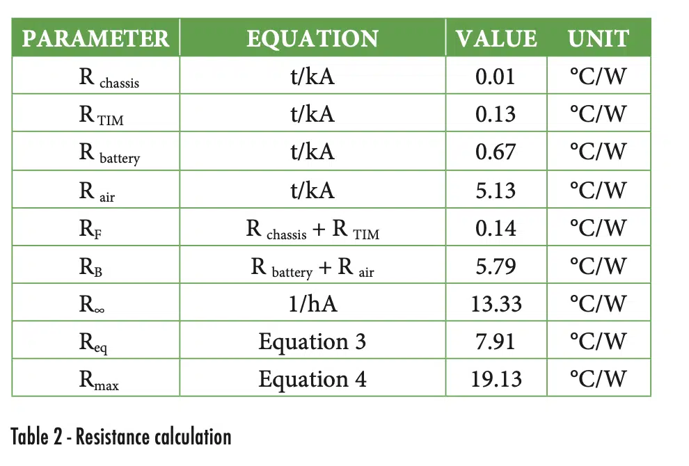
The thermal resistance in each individual layer is calculated using the one-dimensional resistance equation for heat conduction through a medium, t/kA. The resistance to the front and back of the device is calculated by combining the individual layer resistance values; this is achieved via a simple sum when the individual resistors are in series. As an example, the thermal resistance to the front of the device is the sum of the chassis and thermal interface material layers.
The resistance to the environment is calculated using the thermal resistance equation, 1/hA. Note that the effective heat transfer coefficient (h) in this equation must account for all heat rejection modes. In this example, the value is based on the sum of an empirical correlation for natural convection and a linearized radiation heat transfer coefficient.
The total equivalent resistance from the heat source to the environment (Req) of 7.91 °C/W is calculated via Equation 3 and the maximum thermal resistance of 19.13 °C/W is calculated via Equation 4. The maximum thermal resistance occurs through the heat path out of the bottom of the device and is driven by the air gap between the heat source and the battery.
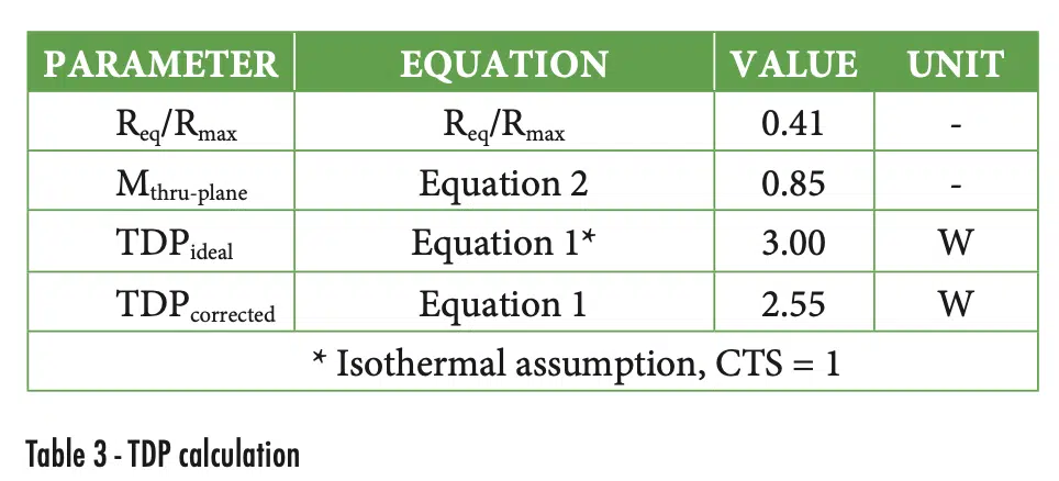
The resulting through-plane multiplier of 0.85 is calculated using Equation 2. Alternatively, the multiplier can be read directly from Figure 3 using the calculated resistance ratio of 0.41 (Req/Rmax). The resulting TDP for the device, when corrected for through-plane thermal gradients, is 2.55 Watts (Table 3). This is lower than the ideal TDP of 3.00 Watts. If additional thermal capability is required, the thermal designer can iterate this process to converge on a more satisfactory set of design parameters (e.g., balance heat paths via through-thickness gaps, materials, etc.).
Concluding Remarks
This first-order method provides the thermal engineer with a tool to quickly estimate the thermal design power limit for devices that experience though-plane thermal gradients. This approach is well suited for architecture studies in which the design rapidly evolves and estimates are needed to guide the design team. While this method can be very useful, it does not replace detailed design and validation. It is instead intended to refine design concepts before transitioning to more detailed simulations and/or tests.
Since real products experience through-plane and in-plane thermal gradients simultaneously, future work is planned to combine the tools provided in Parts 1 and 2 of this column to enable readers to account for both through-plane and in-plane thermal gradients simultaneously in their thermal design power calculations.
References
[1] Victor Chiriac, “A Figure of Merit for Smart Phone Thermal Management”, Electronics Cooling Magazine, April 2017
[2] Frank Incropera and David DeWitt, Fundamentals of Heat and Mass Transfer, 4th Edition, Wiley (1996)
[3] Alex Ockfen, “Calculating Thermal Design Power for Mobile Consumer Electronics – Part 1”, Electronics Cooling Magazine, February 2023
