Overview
Thermal Design Power (TDP) is a term commonly used in thermal management of consumer electronics. While the usage of this terminology may vary across the industry, it commonly refers to the amount of power that a device may dissipate indefinitely, in a given thermal environment, without exceeding the temperature limits of the device. The TDP for a consumer electronics device is of great interest because it provides physical bounds to the experience a product can deliver to the user (e.g., phone call, internet, photo capture, gaming, etc.).
Thermal design engineers often have the most influence on a product’s design during its architecture development. It is not uncommon for designs to rapidly evolve in this phase of the design cycle, with real-time changes occurring daily or even hourly. Some first-order tools are essential to provide effective thermal design guidance in a fast-paced environment. Detailed finite element or computational fluid dynamics simulations are often not practical due to the timeline and lack of design maturity. TDP provides one simple and useful metric that can guide the design in the desired direction.
Where We Left Off
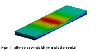
Physics-based methods for determining the thermal design power of a passively cooled consumer electronics device have been developed. The thermal design power of a device like that shown in Figure 1 is typically calculated using equation 1, where h is the effective heat transfer coefficient, A is the external area of the device, Tlimit, is the touch temperature limit, Tambient is the ambient operating temperature, and the CTS is the coefficient of thermal spreading [1]
The coefficient of thermal spreading is a term that accounts for any spatial temperature gradients over the surface of the device. This term is typically between 0.5 and 0.8 for consumer electronics devices, with a value of 1.0 representing the ideal isothermal device.
Part 1 of this column provided a method to calculate the CTS for thermal gradients in the plane of the device [3], while Part 2 provided a method to calculate the CTS for thermal gradients through the thickness of the device [4]. These methods will be briefly summarized in the following sections, then they will be combined to provide the thermal design engineer with a CTS calculation methodology that enables them to simultaneously capture the effects of both in-plane and through-plane temperature gradients on thermal design power.
In-Plane Thermal Gradients
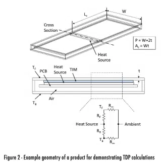
Figure 2 defines the general construction and geometry of the consumer electronics device used to illustrate the thermal design power calculation. While a notional design with the heat source along the centerline of the device is shown here, the approach is general, and the practicing engineer may adjust the parameters to fit their specific needs.
The large aspect ratio of mobile phones and tablets is reminiscent of a fin. Thus, an in-plane coefficient of thermal spreading can be calculated using equation 2, where η is the fin efficiency, Lc is the characteristic length, and m is defined via equation 3.
The quantity m is a function of the fin perimeter (P), cross-sectional area (Ac), effective conductivity of the device housing (keff), and the heat transfer coefficient (h). The heat transfer coefficient in this equation can be chosen using empirical correlations and should account for both convection and radiation.
Through-Plane Thermal Gradients
A through-plane coefficient of thermal spreading can be calculated using a parallel resistance network as shown in Figure 2, where the thermal resistance values from the heat source to the front (RF) and back (RB) surfaces of the device define the heat transfer split and through-plane temperature differential. These resistance values can be calculated using the standard resistance formulas for conduction and convection as provided in equation 4.
Solution of the parallel resistor network yields the thermal spreading multiplier (M*through-plane), defined in equation 5, where R∞ is the thermal resistance between the device surface and the external environment. R∞ is calculated based on the full surface area of one side of the device (front or back only). Note that this multiplier includes the in-plane fin efficiency which is required when in-plane temperature gradients are present and influence resistance to ambient. This fin efficiency parameter was not included in reference [4] because no in-plane temperature gradients were assumed in that effort.
Two additional equations are provided to enable a non-dimensional formulation and enable generic design plots against the quantity Req/Rmax. Req is defined by equation 6 and represents the total equivalent thermal resistance from the heat source to the environment (including both front and back surfaces). Rmax is defined by equation 7 and represents the larger of the thermal resistances between the heat source and the environment (through either the front or back surfaces individually).
Bringing It All Together
It is typically not practical to design a device with either perfect inplane thermal spreading or with a perfect heat balance between the front and back surfaces. Thus, it is useful to extend the equation for the coefficient of thermal spreading to include both the in-plane and through-plane contributions previously discussed.
The combined coefficient of thermal spreading calculation is provided in equation 8 and is obtained by multiplying the fin efficiency (η) from equation 2 and the through-plane multiplier (M*through-plane) from equation 5.
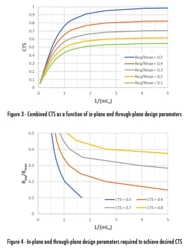
Figure 3 illustrates the coefficient of thermal spreading as a function of the non-dimensional design parameters governing in-plane (1/mLc) and through-plane (Req/Rmax) thermal performance. The CTS is shown to be most sensitive to in-plane thermal spreading and can approach zero when 1/mLc approaches zero. This can occur when either the effective thermal conductivity of the housing becomes small, or the device becomes large (compared to heat source size). The importance of through-plane heat spreading is also apparent as a near-ideal in-plane design (1/mLc = 5) may yield a coefficient of thermal spreading of 0.5 if there is an extreme imbalance in the thermal resistance between the heat source and the front and back surfaces of the device.
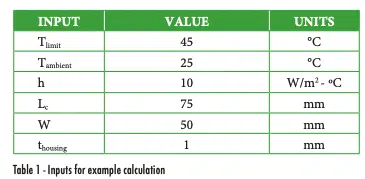
We can now reframe the data to make it more useful for the thermal design engineer. Thermal design power targets are commonly known and can be easily translated into a target CTS value using equation 1. Figure 4 provides design curves for multiple target CTS values. Each curve provides a set of design combinations that can be selected to achieve a target CTS value based on in-plane (1/ mLc) and through-plane (Req/Rmax) design parameters.
We now have all the tools we need to calculate the physics-based coefficient of thermal spreading and enable robust prediction of system thermal design power.
Putting it into Practice
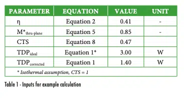
Let’s demonstrate this for the notional device with the inputs specified in Table 1. It is common for the environment, temperature limits, and form factor to be known early in the design process.
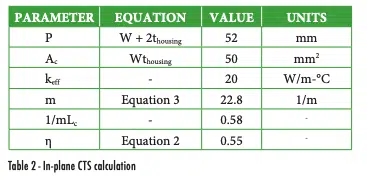
Assuming we use a housing material construction with an effective thermal conductivity of 20 W/m-°C, the in-plane thermal performance is calculated in Table 2. The calculated fin efficiency is 0.55, meaning the device rejects heat from its top or bottom surface as effectively as an isothermal surface with 55% of the area.
The cross-section of the notional device is provided in Figure 5. Heat is assumed to be generated on the heat source located in the middle of the device. Heat leaving the front surface of the device passes through a thermal interface material (TIM) that is the same size as the heat source. Heat leaving the back of the device passes through the printed circuit board (PCB) and an air gap. The thickness (t) and thermal conductivity (k) of each layer is specified in Figure 5.
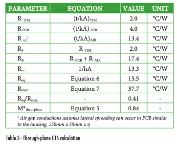
The thermal resistance in each individual layer is calculated using the one-dimensional resistance equation for heat conduction (equation 4). The resistance to the front and back of the device is calculated by combining the individual layer resistance values; this is achieved via a simple sum when the individual resistors are in series. The area used in the PCB and TIM resistance calculations is assumed to be that of the heat source (500 mm2 ).
The resistance to the environment is calculated using the thermal resistance equation for heat convection. Note that the effective heat transfer coefficient (h) in this equation accounts for all heat rejection modes. In this example the value is based on the sum of an empirical correlation for natural convection and a linearized radiation heat transfer coefficient.
Table 2 summarizes the through-plane heat spreading calculation. The ratio of the equivalent resistance to the maximum resistance (Req/Rmax) is 0.41. Given that this value is below 0.5, there exists an imbalance in heat transfer between the front and back surfaces of the device. The resulting through-plane multiplier (M*through-plane) is 0.85.
Now that we have calculated the in-plane and through-plane performance, we combine them in Table 3 to calculate an overall coefficient of thermal spreading of 0.47. The resulting thermal design power for the example device is thus 1.40 Watts. This is much lower than the ideal thermal design power of 3.00 Watts, illustrating the influence of in-plane and through-plane temperature gradients on device capability.
If additional thermal capability is required, the thermal designer can iterate this process to converge on a more satisfactory set of design parameters. Figure 4 can be used to guide the designer in determining the required in-plane and through-plane design parameters to achieve a satisfactory result.
Concluding Remarks
Thermal design power calculations provide powerful data for efficiently exploring the design space and making architectural decisions such as the form factor of the device, the targeted user experiences, material properties, device construction, and the supported thermal environments. A physics-based approach for calculating the thermal design power for a mobile phone or tablet is provided that includes the effects of both in-plane and through-plane thermal gradients. Approaches such as this are helpful when you don’t have historical test data or are exploring new architectures. Additionally, the approach provides actionable data for reverse engineering the thermal requirements of the design to achieve a desired spreading coefficient or thermal design power.
While this method can be very useful, it does not replace detailed design and validation. It is instead intended to enable early design explorations before you transition to more detailed simulations and/or tests.
References
[1] Victor Chiriac, “A Figure of Merit for Smart Phone Thermal Management”, Electronics Cooling Magazine, April 2017
[2] Frank Incropera and David DeWitt, Fundamentals of Heat and Mass Transfer, 4th Edition, Wiley (1996)
[3] Alex Ockfen, “Calculating Thermal Design Power for Mobile Consumer Electronics – Part 1”, Electronics Cooling Magazine, February 2023
[4] Alex Ockfen, “Calculating Thermal Design Power for Mobile Consumer Electronics – Part 2”, Electronics Cooling Magazine, August 2023

