Abstract
The past two decades have seen many approaches to solder fatigue and solder joint life published. This subject has proved difficult as various failure mechanisms are proposed and examined. While these theoretical bases are discussed, it often leaves the end developer in a difficult situation as to how to apply an accurate simulation approach to fatigue failure for a particular package. In this article, one approach is examined and used to evaluate a “typical” metal lid flip chip BGA (ball grid array) package under variation of a few key parameters via a 2-level DOE (Design of Experiment).
The parameters examined in this article are the in-plane thermal expansion coefficient of the printed circuit board (PCB), the lid material, and the temperature range for the BGA environment. The DOE showed that all three individual parameters are statistically significant, as are interaction terms with packaging materials CTEs (coefficients of thermal expansion) and temperature cycle range, ⊗T. Part 1 of this article describes the background information, the simulation model, and the design of experiments. Part 2 will present the results of the simulations and discuss conclusions.
Background
There have been numerous studies to understand and characterize solder used in electronic packaging. Unfortunately, solder’s behavior in electronic systems is anything but simple and linear, which has led to a plethora of research studies that have led to a variety of solder characterization models that are not necessarily in agreement. This provides challenges to standard product development, especially when trying to decide which model(s) should be used.
In addition to selecting a suitable model for solder in order to predict package reliability, designers may have choices in package geometries, materials, and assembly methods that can help reduce solder fatigue from thermal cycling. For example, in a BGA, a smaller die reduces the strain seen at the corner solder bump locations. Reducing CTE mismatches between the lid, substrate, or underlying PCB can also help. Similarly, some lid geometries are more favorable under certain conditions. Applying an underfill to the die or using an appropriate lid adhesive can also be used to reduce solder fatigue. Each of these can improve package reliability but may also be constrained by other environmental conditions or manufacturing methods.
Clearly, many BGA packages are produced and used today. However, optimizing them for long lifetimes in extreme conditions is a daunting task to examine with simulation.
Approach
Given the disparity of fatigue models and approaches to failure prediction, the approach described in this article used a specific model/method selected on the following criteria:
- The theoretical background of failure is sound and examined in the literature, preferably by a number of papers
- Test data are used to verify and/or tune the application of the theory
- Solder material tests are used with proper environment (temperature, strain rates) and geometry (tensile samples, or actual part geometry such as solder balls) to create material models
- Effective and proven published FEA modeling approaches are similar to the solder geometry of the actual problem.
Given this set of criteria, the BGA in this article was examined using the approach enumerated by Syed, Sharon, and Darveaux [8]. That paper fulfills the criteria of (1), (2), and (4). This paper is significantly more expansive and comprehensive in its approach than many other papers in the field by covering these three items in an integrated manner. The solder material models (SAC 305 for solder balls, Sn-2.5Ag for solder bumps) were compiled from published tests and conditions. This study, like Ref. [8] uses creep as the damage criteria for fatigue prediction. Hence, elastic-plastic models are used at a low strain rate along with a creep model chosen for fatigue modeling and suited for the solder location (Garofalo model for SAC 305, and Combined Time Hardening for Sn-2.5Ag) [12]. The advantages and disadvantages of various fatigue models are well summarized in Table 1 of Ref. [6] for the interested reader.
Factors to Limit Solder Fatigue
Since a BGA package is a mechanical system composed of different part geometries, materials, and material behavior, it is reasonable that the assembly can be optimized for solder fatigue life. Also, temperature variations of the assembly contribute to the solder life outside of the mechanical specifications. However, not every item or environment variable is under the control of the designer: material and manufacturing limitations can restrict the variables or range of variables while system-level thermal management capabilities will influence temperature variations.
Controlling the CTE mismatch within the package is the key to maximizing the solder fatigue life. In a typical flip chip BGA, stress in the solder bumps between the die and the substrate is influenced by the different CTEs of silicon and the substrate. Stresses in the solder balls, between the substrate and the underlying PCB are affected by the different CTEs of those materials (especially the corner balls, examined in this work). The lid, which is attached to the substrate via some adhesive or solder, affects both the bumps and balls due to the additional warpage it imposes on the package. Figure 2, from Ref. [9], shows a typical design of such a package.
Examining this geometry, it is clear that the assembly works against itself to simultaneously optimize the fatigue life of both the solder bumps and balls. Given that silicon has a CTE of approximately 2.6 ppm/K, a low CTE substrate is desirable for the solder bumps. However, the solder balls are affected by the CTE mismatch between the substrate and the PCB, so a higher CTE PCB would help the solder balls. The lid CTE and the lid adhesive likewise can be tailored to reduce stresses in either the bumps or balls, but not both at the same time.
Since the CTE mismatches tend to produce a shearing load in the solder bumps and balls, another mitigation is to make them as tall as possible so the shear angle is smaller. Another factor is the size of the chip; if it is large, the amount of thermal expansion/contraction creates more shearing load than a smaller die on the solder bumps and possibly the balls. Finally, since all of the thermal loads are driven by the temperature excursion range to which the BGA is subjected, a lower ⊗T reduces thermal strains and increases fatigue life.
This article addresses a limited set of factors that are less constrained by manufacturing options for a typical BGA. Specifically, it considers a low/high CTE lid, a low/high CTE PCB, and a low/high temperature ⊗T on the system.
Substrate Construction Constraints
A number of interconnected package design drivers influence package warpage that influences solder fatigue. Some of the most common drivers include:
- Signal propagation at high speeds typically requires use of low loss materials, which generally have relatively high CTE.
- High-speed signals must be shielded and grounded to avoid crosstalk. This requires vias and alternating ground and signal layers that can consume substantial substrate real estate as well as additional layers. For example, two high speed routing layers would require a 4-2-4 or 5-2-5 stackup, while three routing layers would require a 6-2-6 or 7-2-7 stackup.
- Common fabrication methods call for significant copper coverage in each substrate layer, often 60-80%, which drives up the substrate’s effective CTE.
- Increasing device bandwidth leads to more high-speed signal lanes, which increases the sizes of both the silicon and package substrate. The larger substrate size, as well as the size of the bump field, exacerbates package warpage.
- Larger devices with more high-speed signals/lanes tend to consume more power, leading to higher temperatures and increased thermal expansion.
- Challenging operational environments and cooling solutions can increase warpage and solder fatigue, if not optimized properly.
The aforementioned drivers can limit options on how the package is constructed, including material choices, thicknesses, and geometry. As these considerations can not necessarily be ignored or considered independently, the package designer must identify the best balance for each package substrate. It is crucial that the packaging engineer be involved in the upstream development of the chip architecture or floorplan to ensure that early decisions do not adversely affect the assembly process. Similarly, the package engineer must also consider the downstream assembly processes to identify warpage-related requirements and methods to compensate for warpage. A good example of this is thermal/CTE compensation, in which the substrate bump field is pre-shrunk so that the bumps align, mate, and lock with the silicon when at the assembly temperature. The successful package engineer considers multiple disciplines and teams (physical design, mechanical, SI/PI, manufacturing partners/vendors) to drive the substrate to successful fabrication and assembly.
Sample BGA Model and Problem
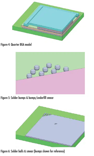
A simple JEDEC standard BGA was modeled for this analysis. This is a one quarter model where symmetric boundary conditions are applied to the center surfaces. The model uses a standard JEDEC substrate board size (33×33 mm), 0.8 mm pitch solder balls, and 100 µm solder bumps between the substrate and the single 20x20mm die. The corner bump under the die is removed, which is often done for large die manufacturing. For these simulations, only some of the individual solder bumps and balls were discretely modeled. To reduce mesh size, the majority of solder bumps/balls were modeled as layers with orthotropic smeared material properties. The bump smear was a solder/underfill composite while the ball smear was a composite of solder and air. Figures 4-6 show the solid quarter model geometry.
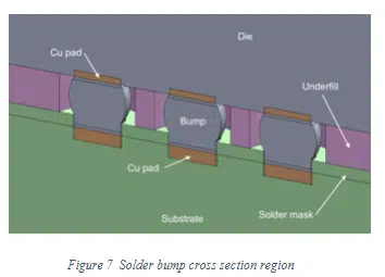
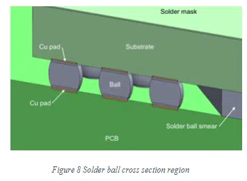
The geometric shapes of the modeled solder bumps and balls were accurate. However, these volumes were sliced so that the damage in the most critical areas, namely the tops and the bottoms of the bump/ball, could be calculated. The stress that initiates fatigue cracks occurs in these critical regions. The average damage in these portions of the solder correlates much better to the cycles to failure than the average damage over the entire bump/ball volume. Critical regions in the model were defined by 5µm slices on the top and bottom of each bump while solder balls included 25µm slices. Each bump/ball was attached to a copper pad at the top and bottom, which induces the CTE mismatch. The intermetallic layer (IMC) was not modeled, as it has shown in other studies to not significantly affect reliability predictions. Figures 7 and 8 show the detailed geometry of the bumps and balls used in this study.
Design of Experiments
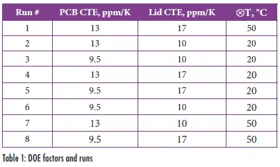
Since the simulations examined three variables (lid CTE, PCB CTE, and the system ⊗T) over a high/low range, a simple 2-level 3-factor DOE was used to create the simulation matrix. This required 8 simulations runs (2³) along with an additional finer mesh simulation to validate mesh resolution. A full DOE identifies statistically significant variables and interactions, as well as the relative importance of variables. The test matrix produced outputs for the cycles to failure for both the solder bumps and solder balls. Those results are evaluated independently, so the identified significant variables and interactions may not be the same.
Table 1 shows the values of the parameters used in the DOE matrix. Values represent typical BGA manufacturing operating conditions, but with different material choices or operating environments, they easily could be larger/farther apart. Larger variable ranges would be better covered with a 3-level DOE.
The environmental cycle condition of 20°C or 50°C was applied to the entire BGA assembly. The die is not heated in this case (although it can be for actual problems). One thermal cycle was defined as a two-hour period with 15-minute dwell times at each extreme, and 45 minutes to traverse from one temperature to the other.
Conclusion
This article is part of a two-part series of articles based on Ref. 11. Part 2 of the series will describe the simulation software used, the mathematical model used for the solder, the analysis details, the statistical analysis of the DOE results, and conclusions drawn from the study, along with other details used in Part 1 of this article.
Authors
James Petroski is the owner of Design by Analysis Technical Consulting LLC. He has worked in the area of electronics packaging for nearly 40 years and has a special focus on thermal and mechanical engineering of packages and electronic systems. His background includes equipment design for naval nuclear propulsion instrumentation and controls, NASA space flight experiments (with three shuttle flights of space hardware), computer systems/enclosures, handheld commercial and industrial products, graphite thermal materials and applications, LED lighting systems, and packaging of die and die/substrate systems. He received his Bachelor’s in Engineering Science and Mechanics from Georgia Institute of Technology (Georgia Tech) and an MS degree in Engineering Mechanics from Cleveland State University.
Andy Carrasco has worked in electronic circuit design and semiconductor packaging for 27 years. He worked the first half of his career in EDA developing custom IC package design tools. He co-founded nSentia in Japan to pioneer an acclaimed IC package visualization and assembly verification tool. Since 2012, he has consulted on numerous hardware development projects, specializing in complex advanced IC package substrates, with a particular focus on large body, high-speed, high-power, 2.5D devices, the last 5+ years at Cisco Silicon One. Throughout his career, he has focused attention on blending electronics engineering with mechanical modeling. He holds an undergraduate degree from Temple University Japan.
References
[1.] Lee, W. W., Nguyen, L. T., & Selvaduray, G. S. (2000). Solder joint fatigue models: review and applicability to chip scale packages. Microelectronics reliability, 40(2), 231-244.
[2.] Chen, G., Zhao, X., & Wu, H. (2017). A critical review of constitutive models for solders in electronic packaging. Advances in Mechanical Engineering, 9(8), 1687814017714976.
[3.] Mukherjee, S., Nuhi, M., Dasgupta, A., & Modarres, M. (2016). Creep constitutive models suitable for solder alloys in electronic assemblies. Journal of electronic packaging, 138(3), 030801.
[4.] Depiver, J. A., Mallik, S., & Amalu, E. H. (2020, September). Comparing and benchmarking fatigue behaviours of various SAC solders under thermo-mechanical loading. In 2020 IEEE 8th Electronics System-Integration Technology Conference (ESTC) (pp. 1-11). IEEE.
[5.] Su, S., Akkara, F. J., Thaper, R., Alkhazali, A., Hamasha, M., & Hamasha, S. D. (2019). A state-of-the-art review of fatigue life prediction models for solder joint. Journal of Electronic Packaging, 141(4), 040802.
[6.] Gabriel, O. E., and Huitink, D. R. (October 22, 2022). “Failure Mechanisms Driven Reliability Models for Power Electronics: A Review.” ASME. J. Electron. Packag. June 2023; 145(2): 020801.
[7.] Basit, M., Motalab, M., Suhling, J. C., & Lall, P. (2015, July). Viscoplastic constitutive model for Lead-free solder including effects of silver content, solidification profile, and severe aging. In International Electronic Packaging Technical Conference and Exhibition (Vol. 56895, p. V002T01A002). American Society of Mechanical Engineers.
[8.] Syed, A., Sharon, G., & Darveaux, R. (2012, May). Factors affecting Pb-free flip chip bump reliability modeling for life prediction. In 2012 IEEE 62nd Electronic Components and Technology Conference (pp. 1715-1725). IEEE.
[9.] Lau, John H., (April 13, 2022). Recent Advances and Trends in Advanced Packaging. Presented at IEEE EPS Binghamton Chapter (slide 11)
[10.] Syed, A. (2004, June). Accumulated creep strain and energy density based thermal fatigue life prediction models for SnAgCu solder joints. In 2004 Proceedings. 54th electronic components and technology conference (IEEE Cat. No. 04CH37546) (Vol. 1, pp. 737-746). IEEE.
[11.] J. Petroski and A. Carrasco, “Simulation of Solder Fatigue Effects on Typical BGA Package due to Material and Temperature Variations,” 2024 40th Semiconductor Thermal Measurement, Modeling & Management Symposium (SEMI-THERM), San Jose, CA, USA, 2024, pp. 36-45.
[12.] There are many dozens of papers with models considered, and each problem involves choosing the model best suited to the problem. One example of a good reference in this area is: Depiver, Joshua A., et al. “Creep damage of BGA solder interconnects subjected to thermal cycling and isothermal ageing.” 2019 IEEE 21st Electronics Packaging Technology Conference (EPTC). IEEE, 2019.
