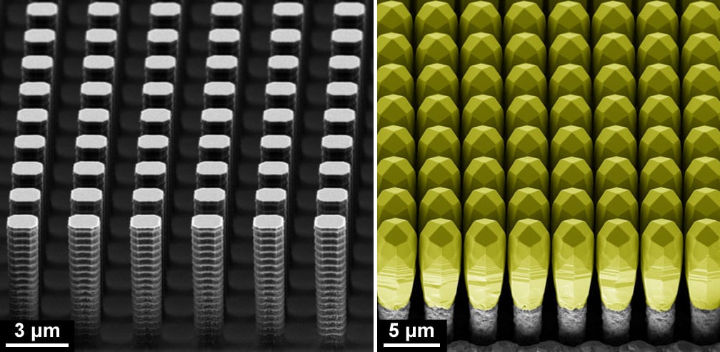
Germanium grown epitaxially on micrometre-sized silicon pillars forms perfect crystals free of defects. The resulting Ge/Si “virtual substrate” is lighter and tougher than a free-standing Ge substrate and clears a path towards high-resolution CMOS X-ray detectors and high-efficiency multi-junction solar cells for both space and terrestrial applications.
Micrometre-scale layers of pure Ge are attractive for infra-red photodetectors, the final layer of triple-junction solar cells, or as “virtual substrates” for the deposition of GaAs-based layers. Increasing the Ge thickness still further (to several tens of micrometres) would enable the realisation of X-ray and particle detectors which are more efficient than their existing Si-based counterparts. The increased efficiency coupled with the good compatibility between Ge and Si leads to the final goal of a pixel detector in which the Ge absorbs the photons or particles and the resulting signals are handled by Si CMOS readout electronics.
The growth technique of low-energy plasma-enhanced chemical vapour deposition (LEPECVD) [3] has led to the efficient and fast deposition of such layers, but, once the Ge layer is more than a few micrometres thick, the thermal contraction during the cooling of the substrate back to room temperature after growth causes bending of the substrate and cracking of the Ge layer.


