INTRODUCTION
A Thermal Load Board (TLB) is a hardware tool used to simulate an actual application board, for example – computer motherboard, blade server board, handheld device main logic board, etc. Mounted on the TLB are a variety of heat source simulators that allow heat flux generation in a manner that closely approximates real semiconductor devices and other components mounted on the application board in terms of physical size, heat flux magnitude, and heat flux flow patterns. Temperature and air flow sensors can be mounted on the TLB for monitoring purposes and for calibraton of thermal simulation results.
The benefits of using a TLB are summarized as follows:
– Reduced electronic system development costs.
System developers can zero in on a thermal management design much more quickly. The TLB is a tool that can be designed and fabricated relatively fast. The alternative is waiting for the application board to be electronically completed and available, and then instrumented for temperature sensing, for use in thermal management design projects. Turn-around time from initial design input to completed TLB is in the four to six week [C1] range and variations from the first to next TLB can be as short as three to four weeks.
– Improved system operational and reliability performance
A properly designed TLB will provide thermal management designers an opportunity to generate a variety of heat flux levels to simulate various power loading conditions in both static and transient modes, thus allowing for better thermal management optimization. Short turn-around time for TLB revisions allows for relocation of heat sources to better optimize the thermal management. Lower semiconductor junction and electronic component temperatures translate directly to better system operation and reliability.
– Reduced time to market
New product introductions are timed to either carve out a market niche before competition arrives, to react to competitive products already in the market, or to protect the market position of predecessor products already in the market. The term is usually defined as “time to market (TTM) is the length of time it takes from a product being conceived until its being available for sale.”[1] In general, the thermal management design usually starts well after the product development project has begun because there is too much of the system design still in flux in the early part of the project to make thermal design efforts worthwhile. However, application board outline dimensions, general heat source spatial locations, and design power levels are usually known early in the product development cycle. This information is sufficient to construct a TLB that can be put to use well before the application board is finalized.
DESIGN CONSIDERATIONS
The design considerations required for starting a TLB development and fabrication project falls into five groups
Physical Dimensions
The TLB must match the application board in all X, Y & Z dimensions, including cutouts, protrusions, and critical mounting holes. The Z dimension refers not only to the thickness of the application board but also the height of components, modules and semiconductor devices mounted on the board. If the product design calls for modules or “daughter-boards” to be mounted on the TLB and these elements affect the thermal management design, then the physical dimensions of and mounting instructions for these elements must also be provided.
Power Loading and Heat Flow
The key to designing a TLB that effectively mimics the thermal performance of an application board lies in the design and implementation of the heat sources. Not only must the heat sources match the dimensions, location on the TLB and power dissipation of actual components and semiconductor devices mounted on the application board but they also must closely approximate the heat flow into the mounting surface and into the environment and/or the thermal management solution.
There are several ways of generating heat flux on the TLB to simulate active components on the application board. The most common practice is to use either resistors or diodes in surface mount packages. Transistors (MOSFET or Bipolar) can also be used but powering up these devices is more complex because of the active nature of power dissipation in these devices. Surface mount resistors (usually referred to as chip resistors) are available in 1206 surface mount devices SMD packages that are approximately 3.2mm X 1.6mm X 0.55mm and will dissipate 0.25W and comparable diodes are available in MicroSMP packages that dissipate 0.5W. These small devices can easily be arrayed to dissipate power in the range of a few hundred milli-Watts to greater than 10 Watts, depending on the array area.
If higher power levels are required, the next choice is metal foil resistors encapsulated in electrically insulating films, such as KaptonTM with connecting wires protruding from one edge. These heaters are relatively thin and are available in a variety of X-Y dimensions. Power dissipation in the 8W range is possible in a 1cm X 1cm size.
At even higher power dissipation levels, the best choice is to use a Thermal Test Chip (TTC) either directly mounted on the TLB or mounted in a package and then the package is mounted on the TLB. The latter configuration is typically referred to as a Thermal Test Vehicle (TTV). TTVs are sometimes available from larger semiconductor manufacturers but are often hard to obtain. An alternative is third-party TTC suppliers that can either provide the chip itself or mount them in a suitable package[C2] .
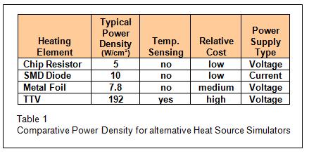
Table 1 shows a comparison between various approaches to TLB heat flux generation for Heat Source Simulators (HSS). The Diode approach requires a constant current supply for power generation because of the diode’s negative temperature coefficient – if a voltage is applied the current will continue to increase until a steady state condition occurs or the diode destroys itself. It is possible to obtain metal foil heater with an integrated temperature sensor but then the power density capability decreases, the cost increases, and the delivery time becomes much greater. The TTV, while providing the closest approximation to an actual semiconductor component, has the highest relative cost and may not be easily available in same package style as the actual component it is simulating.
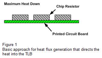
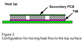
After selecting the approach for generating the heat flux, the next consideration is establishing the heat flow configuration. Figure 1 shows the basic configuration of mounting chip resistors or diodes directly onto the TLB. In this case, nearly all the heat flow is directly into the TLB. If heat flow is desired in the upward direction, this can be accomplished using the configuration shown in Figure 2 where the chip resistors or diodes are mounted on a thin printed circuit board (PCB) and then mounted upside down on the TLB. The amount of heat flow into the TLB can be controlled by the thermal conductivity of the Thermal Interface Material (TIM) or by insertion of thermal insulation material. Either of these two approaches are applicable if controlling the height (Z direction) of the heat source simulator is not critical.
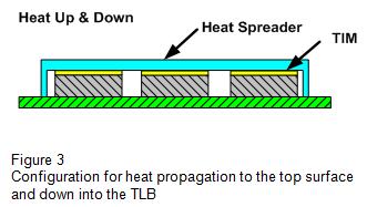
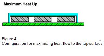
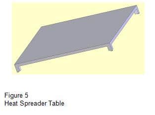
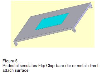
If HSS height is an important requirement, such as in the case of a thermal management solution that must conduct heat from several different heat source on the TLB, the configuration shown in Figure 3 provides a good solution. Here the height can be precisely controlled by the thickness of the heat spreader core and the length of the heat spreader legs. Heat is conducted to the bottom of the heat spreader core through the TIM. To maximize heat flow into the heat spreader core and, hence in the upward direction, the chip resistors or diodes can be mounted on a small, thin PCB and that assembly mounted upside down on the bottom of the heat spreader core as shown in Figure 4. The air gap between the chip components and the TLB minimizes heat flow in that direction. If some heat flow into the TLB is desired, then TIM can be inserted instead leaving an air gap. An alternative approach is to increase the X-Y dimensions of the heat spreader legs. Small protrusions at the end of the legs, as shown in Figure 5, can be inserted into holes on the TLB to facilitate exact positioning of the heat spreader on the TLB. If the heat source simulator is to simulate a semiconductor package that has a metal lid that is smaller than the package footprint or to simulate a Flip Chip (i.e., bare die) package, the heat spreader can be designed with a pedestal to match the X-Y dimensions of the thermal interface surface as shown in Figure 6. The configurations shown in Figures 3 and 4 can also be implemented with metal foil heaters. However, these heaters work best when sandwiched between two flat surfaces and when there is room to run the wires to them.
For a better approximation of an actual semiconductor heat producing component, the obvious choice is the TTC in a package that reasonably approximates that of the actual semiconductor unit. This TTC approach can offer non-uniform heating flexibility and the opportunity to measure temperatures in single or multiple locations that is indicative of the actual semiconductor unit junction temperatures[C3] .
Board Construction:
The TLB must closely approximate the thermal characteristics of the application PCB. However, most application PCBs have many copper layers, – 12 to 18 layers or more is common for complex blade servers or computer motherboards. Designing a TLB with a comparable number of layers would significantly increase the TLB development time and fabrication cost. The alternative is to design the TLB with only four layers – top, bottom, and two internal planes – that have copper areas and thicknesses that are thermally equivalent to an application board with many more layers.
Most application PCBs used in non-extreme environmental conditions are fabricated from FR-4 epoxy fiberglass dielectric material or variants based on the same or similar material composition. The thermal conductivity of this type of material is relatively low – about 0.4W/m-K[C4] . The thickness of each dielectric layer in combination with the thickness of the copper layers must match the total thickness of the application PCB.
Vias in the board must also be considered, especially if some or all are intended for thermal conduction. As an example, via connections to an internal copper plane are necessary for packages that have thermal pads or balls. However, “blind” vias – those that do not go through the board – are usually not implemented in a TLB because of added fabrication complexity and associated cost. The size and construction of the thermal vias are designed to closely approximate the thermal performance of those on the application board.
Temperature Measurement:
Thermal simulation model calibration requires knowledge of temperature values at specific locations on the TLB. For this reason, it is important to determine exactly where the temperature sensors should be placed on the TLB. Typical locations are immediately adjacent to the HSS footprint, on the backside of the board under the HSS, in the center of the heat spreader (if used), or the junction of the TTV HSS. Another location often used is in the air flow inlet side of the board.
Temperature sensors typically are either thermocouples, thermistors, diodes or TTV diodes. Thermocouples are the easiest to use but require special wiring and connectors. Diodes are available in very small packages (e.g. – SOT-23) that can be mounted like any other component but require a very small constant current for activation as do the diode temperature sensors built into the TTVs. For most cases, the thermistor is the best choice and they are available in a variety of physical sizes and resistance values[C5] .
Electrical Interconnect
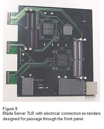
TLBs are almost always designed to go into some kind of enclosure – system rack, computer enclosure, notebook case, game console, etc. The issue of electrical connection to the TLB becomes an important consideration because the physical implementation of the electrical connections should not materially affect the thermal operation of the TLB. For example, using a relatively large connector that restricts air flow or using large gauge wires terminated near a HSS will be difficult to thermally model and should be avoided. Figure 7 shows an example of mounting an extender board on a TLB so insertion of the TLB into a notebook computer case requires passing the TLB Extender Board through a thin slot in the case. Once in place, the clearance around the Extender Board in the slot can be covered with tape to minimize air flow. The end of the board has edge finger traces for interfacing to a standard card connector. An example of Blade Server TLB implementation is shown in Figure 8. In this case, the number of electrical connection required for separate control of each HSS mounted on the board required that four connection extensions be used and each of them had to pass through the front panel. The high current connection requirements dedicated that thin connectors[C6] be mounted at the end of each extension. The ones shown are boxed header connectors that are about 5mm thick. Another approach is shown in Figure 7; the edge fingers on the right only add about 0.1mm to the TLB thickness.
The usual practice in TLB development is to provide a separate electrical connection to each HSS. This provides the maximum flexibility for the user if HSS power levels are not static or if impact of increased power dissipation in one HSS might affect overall thermal performance.
CONCLUSION
The value of a properly designed and implemented TLB has been demonstrated many times over as they have found wide use in industry. The key to proper design and implementation is careful attention to many details, good communications between the TLB provider and the requestor, and shared knowledge of the intended application environment. The references below provide more detailed information on TLB design and implementation [2] [3].
[1]Wikipedia (en.wikipedia.org/wiki/Time_to_market)
References
[2] Siegal, B., “Thermal Load Boards Improve Product Development Process“, IMAPS Thermal ATW 2010
[3] Siegal, B., “Thermal Load Boards – Another Thermal Management Design Tool”, Proceedings of SEMI-THERM 25, San Jose, CA, March 2009

