In this issue, we examine heat flow in a printed circuit board (PCB), which typically is a layered composite consisting of copper foil and a glass-reinforced polymer (FR-4).
A cross-sectional view of such a laminated structure is illustrated in Figure 1. The Figure indicates the numbering system that will be used for indicating the different layers, numbered 1 through to N.
Figure 1: Cross-sectional area of PCB.
In many thermal calculations, it is convenient to treat such a layered structure as an homogeneous material, with two different effective thermal conductivities: one describing heat flow within the plane (In-Plane) and another for heat flow through the thickness of the plane (
Through).
The equations for calculating each of these conductivities, given the values for the thickness and thermal conductivity of each layer, are presented below:
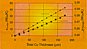
The calculated values of these two quantities are presented in the graph below. In this calculation, it is assumed that the total PCB thickness is 1.59 mm and that the layers consist only of copper and FR-4, with thermal conductivities 390 and 0.25 W/mK, respectively.
It is clear from this graph, that, even for relatively thin layers of copper, (In-Plane) is much greater than (
Through). The graph demonstrates two facts about heat transfer in PCBs.
| 1. | Due to the low thermal conductivity of the FR-4, once a continuous copper path is established in the direction of heat flow, it dominates the heat transfer in the PCB, and |
| 2. | Thermal conduction is not very efficient for heat flow in a direction lacking a continuous copper path. |
Care must be applied in determining which copper layers should be included in these two equations. Only those layers that are capable of spreading the heat a significant distance from the heat source should be included. When PCBs are added, an empirical study has shown that, of the copper layers only the planes should be included [1,2]. For a JEDEC-standard test PCB, on the other hand, the trace layers should be included, since they are routed to the edges of the metallized area of the PCB. In this case, the conductivity of a trace layer would be calculated from the
formula i = fi
Cu, where fi is the fractional coverage of copper in that layer.
A typical PCB used in a personal computer, might have 2 internal copper planes and two outer trace layers. If each of these layers has a thickness of 35 µm (1 oz/ft2 Cu), the total equivalent thickness of the copper would be 70 µm and the values of In-Plane and
Through would be 17.4 and 0.26 W/mK, respectively. Hence, it is clear that in most electronic applications,
In-Plane of the PCB is much less than that of a solid plate of copper. The results show that a typical PCB is not an efficient conductor of heat, leading to significant local variations in the PCB temperature in the vicinity of heat-generating components.
References
| 1. | J.E. Graebner, “Thermal Conductivity of Printing Wiring Boards”, Technical Brief, Electronics Cooling Magazine, Vol. 1, No.2, October, 1995, p. 27. |
| 2. | K. Azar and J.E. Graebner, “Experimental Determination of Thermal Conductivity of Printed Wiring Boards,” Proceedings, SEMI-THERM XII Conference, March, 1996, pp. 169-182. |


