Application of Diamond Heat Spreaders
for the Thermal Management of GaN Devices
Thomas Obeloer*, Bruce Bolliger
Element Six Technologies
3901 Burton Drive, Santa Clara, CA 95054
*thomas.obeloer@e6.com
Yong Han, Boon Long Lau, Gongyue Tang, and Xiaowu Zhang
Institute of Microelectronics, A-STAR, Singapore.
- Introduction
As devices become smaller, they still require high reliability in the presence of extreme power densities (greater than 1 kW/cm2). This creates demand for new thermal management solutions. Nowhere is this more evident than with the use of gallium nitride (GaN) transistors, where engineers struggle with thermal barriers that limit the ability to achieve the intrinsic performance potential of GaN semiconductor devices. Emerging as a common solution to this GaN thermal management challenge are metallized chemical vapor deposition (CVD) diamond heat spreaders [1].
GaN-based transistors and their related radio frequency (RF) power amplifiers (PAs) have emerged as the leading solid-state technology to replace traveling wave tubes in radar, electronic warfare (EW) systems and satellite communications. However, the operation of GaN high electron mobility transistors (HEMTs) on silicon chips poses a significant challenge to thermal management, as the heat generation is concentrated in very small areas, typically measured in microns. The gate-to-gate spacing in typical GaN HEMT devices is typically less than 50 µm. This leads to significant thermal gradients and high operating temperatures, which can affect device performance and endurance. Elevated temperatures adversely impact reliability. As a consequence, effective thermal management is essential for the GaN device and is important to reach its full potential [2]. As found in previous studies, both micro-channel and micro-jet heat sinks can dissipate high heat fluxes anticipated in high power electronic devices [3]. Dissipating the high concentrated heat flux requires an effective heat spreading capability. CVD diamond heat spreaders are particularly suited for such applications [4].
This article assesses the thermal performance of CVD diamond heat spreaders for a hybrid silicon micro-cooler used to cool GaN devices. Several different grades and thicknesses of microwave CVD diamond heat spreaders, as well as various bonding layers, are characterized for their thermal effects. The heat spreader is bonded through a thermal compression bonding (TCB) process to a silicon thermal test chip designed to mimic the hotspots of eight GaN devices. The heat dissipation capabilities are compared through experimental tests and numerical simulations. It is hoped that the findings presented in this article can highlight the potential effectiveness of CVD diamond heat spreaders, utilized in a number of different configurations, for the thermal management of GaN devices.
- CVD Diamond
Diamond possesses an extraordinary set of properties, including: the highest known thermal conductivity, stiffness and hardness; high optical transmission across a wide wavelength range; low thermal expansion coefficient; and low density. These characteristics can make diamond a material of choice for thermal management to significantly reduce thermal resistance in a variety of applications. CVD diamond is now readily commercially available in different grades with thermal conductivities ranging from 1000 W/m-K to 2000 W/m-K. CVD diamond also has fully isotropic characteristics, enabling enhanced heat spreading in all directions.
Ongoing development in the technologies to synthesize CVD diamond has enabled this material to become readily available in volume costs of approximately $1/mm3. In some instances, diamond heat spreaders enable system operation at elevated temperatures, enhance the heat removal capability and reduce the overall system cost. When applied with appropriate die-attach methods, diamond heat spreaders provide reliable solutions for semiconductor packages with significant thermal management challenges [2].
- Experimental Setup
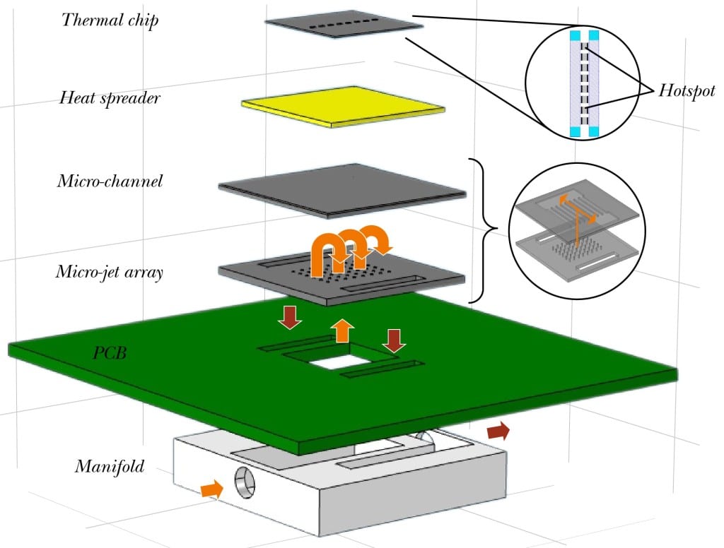
Experiments and simulations will demonstrate the enhancement of heat dissipation capabilities of using CVD diamond heat spreaders in combination with a silicon-based hybrid micro-cooler. Figure 1 shows the experimental setup. A customized test chip exhibiting eight small hotspots was fabricated and bonded to both the silicon cooler and diamond heat spreader through a thermal compression bonding (TCB) process. The silicon hybrid micro-cooler combines micro-jet impingement and micro-channel flow. Different types of CVD diamond material with thermal conductivities of 1500 W/m-K and 2000 W/m-K were attached to the device and their performance compared. Also studied was the thermal effect of both the heat spreader and bonding layer thickness. For the simulated GaN device, the dissipated power densities for various cooling solutions were evaluated.
Figure 1: Schematic representation of the experimental set-up.
The experimental tests were performed on the thermal test chip of 200μm thickness. The chip heating power ranged from 10W to 100W generated by the eight hotspot heaters (each of size 450 × 300μm2). The micro-cooler flow rate was 400 ml/min requiring a pumping power is 0.2W.
4.0 Numerical Model
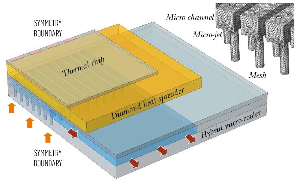
Numerical thermal simulations for the test configuration were performed using commercially available finite element software [5]. Taking advantage of the symmetries in the system, only a quarter of the structure was modelled with symmetrical boundary conditions applied, as is illustrated in Figure 2. Silicon thermal conductivity was modelled as temperature dependent using the relationship:
ksi = 152×(298/T)1.334 (1)
where T is temperature (K) and ksi is thermal conductivity (W/m-K).
The thermal conductivity of the applied solder material, Eutectic Gold/Tin (Au/Sn), is assumed to be constant at 57 W/m-K [6]. The Au/Sn bonding layer of 5μm thickness is assumed between silicon and diamond contact interfaces. Chip heat fluxes are prescribed on the hotspot heaters only.
Figure 2: Quarter geometry numerical model (with the micro-channel cooler in blue).
- Results
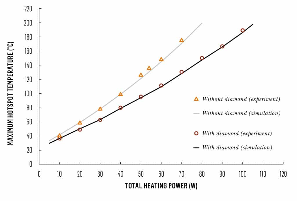
A comparison of measured and predicted maximum chip temperature is shown in Figure 3 for structures with and without a diamond heat spreader. Overall, it is observed that experimental measurements and numerical predictions are in close agreement.
Figure 3: Comparison of measured and predicted maximum chip hotspot temperature for different heating powers with and without a diamond heat spreader.
Without the diamond heat spreader, the structure can dissipate 30W heating power (hotspot heat flux 2.8 kW/cm2) and 70W (6.5 kW/cm2), while maintaining the maximum hotspot temperature (as measured at the die surface) under 80ºC and 180ºC, respectively. With the diamond heat spreader, the heat dissipation is improved significantly to 5 kW/cm2 (for 54W) and 6.5 kW/cm2 (at 70W heating power). Maximum hotspot temperature is reduced by approximately 26% in both cases. To maintain the chip temperature under 180˚C, the structure having the diamond heat spreader can dissipate around 100W heating power (hotspot heat flux 9.2 kW/cm2). Without diamond, power dissipation is reduced to 70W.
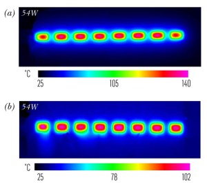
For chip power dissipation of 54W (5 kW/cm2), the measured temperature distribution on the top chip surface is shown in Figure 4, for cases using and not using a CVD diamond heat spreader. The maximum temperature of the measured hotspot located near the chip edge is 8ºC lower than in the center of the structure without diamond heat spreader. Including the diamond heat spreader results in a 2ºC peak temperature differences between the hotspots located near the chip edge and center.
Figure 4: Measured infrared thermographs of the heating areas on the thermal test chip (a) without and (b) with diamond heat spreader for 54W power dissipation. The maximum scale value reflects the peak temperature.
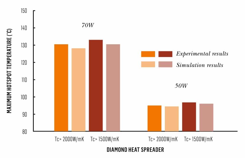
The experiment was repeated using a diamond heat spreader having a lower thermal conductivity of 1500 W/m-K rather than 2000 W/m-K. As observed in Figure 5, for the same power dissipation, the change in the maximum hotspot temperature rise using diamond having a thermal conductivity of 1500 W/m-K is within 2% of that for 2000 W/m-K.
Figure 5: Comparison of measured and predicted diamond heat spreader thermal performance as function of thermal conductivity and chip power dissipation.
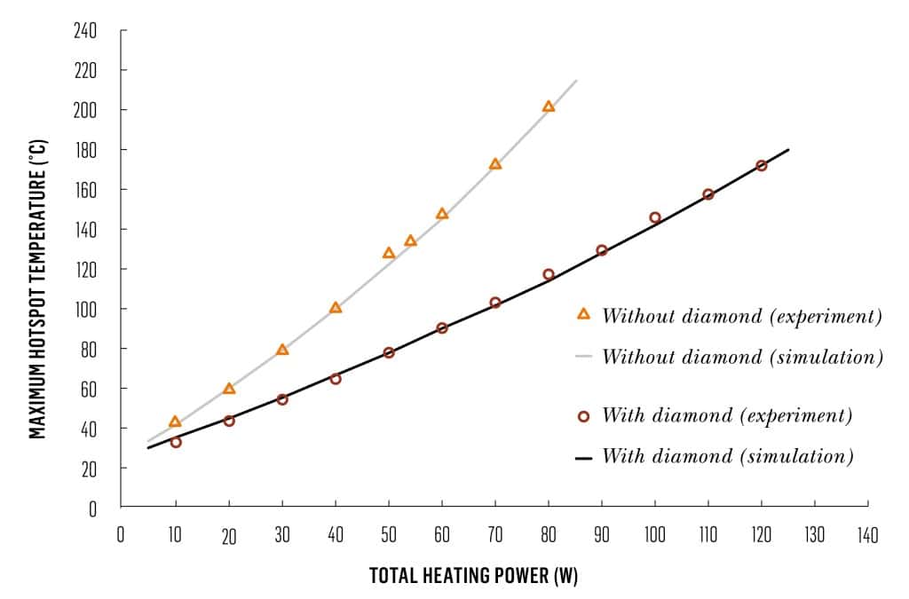
Additional experimental tests and simulations were conducted on a thermal test chip of 100μm thickness. Figure 6 shows the comparison results of the thermal effect. Compared with the results in Figure 3, without the diamond heat spreader, only a slight temperature decrease is enabled by reducing the chip thickness from 200μm to 100μm. For 70W heating, the maximum temperature decreases by less than 2%. However, using a chip thickness of 100μm, with smaller thermal resistance between the heat source and the heat spreader, will improve heat dissipation. The diamond heat spreader can dissipate 110W of heating power (10.2 kW/cm2) while maintaining the maximum hotspot temperature under 160ºC. To dissipate 70W heating power, the diamond heat spreader can reduce by 40% the maximum hotspot temperature. It should also be noted that when using the CVD diamond, the heat flux distribution on the top surface of the silicon micro-cooler for the structure significantly changes. The maximum heat flux is reduced from 2.66kW/cm2 to about 0.39kW/cm2. The maximum thermal resistance of the whole cooling structure, which is related to the total heating power and the maximum temperature of the cooling structure, can be reduced by 73% using the diamond heat spreader for the hotspot thermal management.
Figure 6: Maximum hotspot temperature as a function of heating power with and without the diamond heat spreader having a thermal conductivity of 2000 W/m-K.
- Spreader thickness investigation
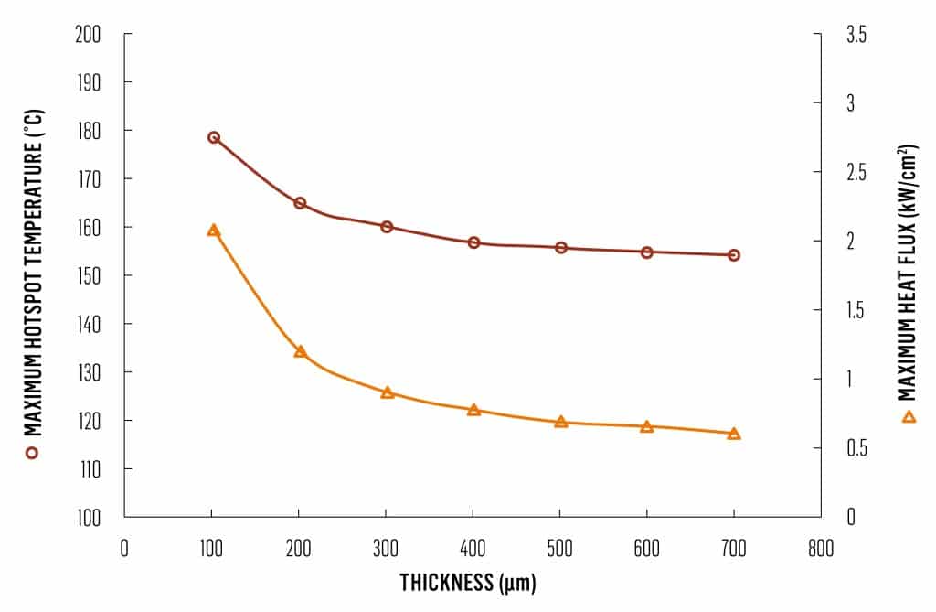
Additional simulations were performed to investigate the effect of the diamond heat spreader having a thermal conductivity of 2000 W/m-K and thickness ranging between 100μm and 700μm. Figure 7 illustrates the variations of the maximum hotspot temperature and the maximum heat flux at the top surface of the silicon micro-cooler.
Increasing heat spreader thickness will cause a reduction in temperature and heat flux. The thermal performance is only slightly improved by increasing the thickness from 400μm to 700μm, but is more pronounced in the thickness range between 100µm to 400μm, where the maximum hotspot temperature and the heat flux can be reduced by around 12% and 63%, respectively. Changing heat spreader thickness will also affect the temperature distribution. For 110W power heating, the peak temperature variation rates of the hotspots are 6.9%, 3.2% and 2.6% for heat spreader thicknesses of 100μm, 400μm and 700μm, respectively.
Figure 7: Predicted effect of diamond heat spreader thickness having a thermal conductivity of 2000 W/m-K on the thermal performance of the cooling structure having 110W power dissipation.
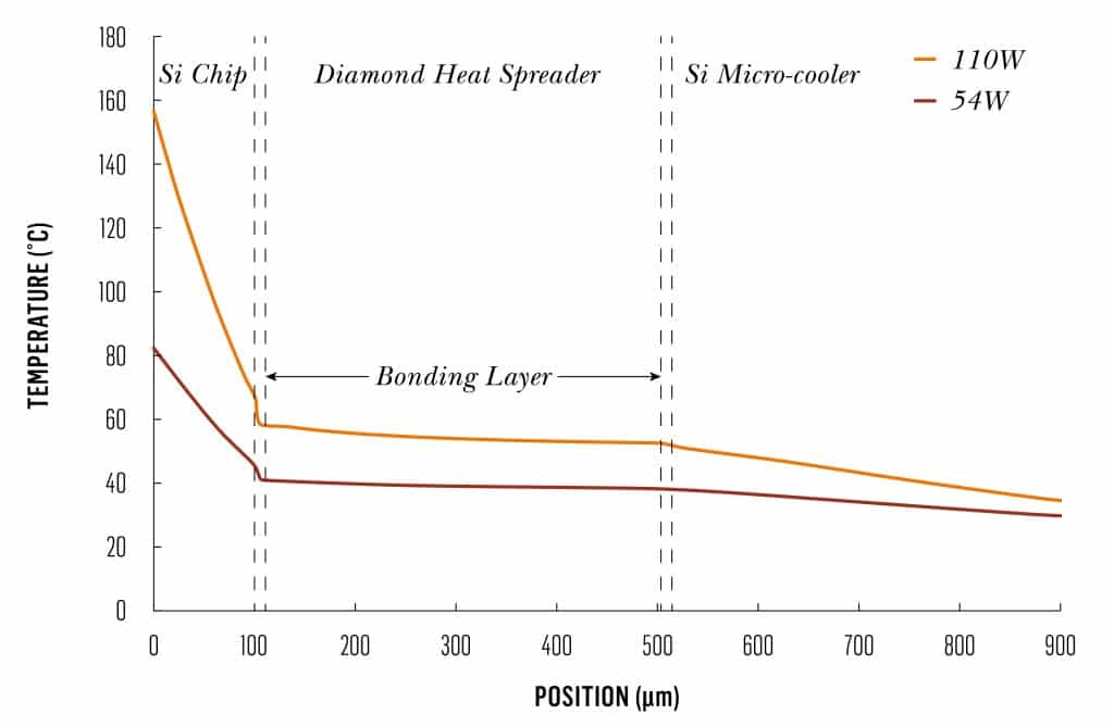
The component assembly (Figure 1) has two bonding layers, one between the chip and heat spreader and the other between micro-cooler and heat spreader. These layers are critical to assure low thermal resistance. In the experimental tests, the thickness of both bonding layers is approximately 5μm. Figure 8 shows the predicted temperature profile vertically from the silicon thermal chip to the micro-cooler. To dissipate 110W power, the temperature rise caused at the chip-diamond bonding layer is around 8.1ºC, while at the diamond-cooler bonding layer the temperature rise is negligible. The bonding layer on the topside of the heat spreader, being much closer to the heat source, has a stronger effect on the hotspot cooling. Additional simulations show that the thermal performance is quite sensitive to the thickness of the bonding layer at chip-diamond interface. By increasing the thickness from 5μm to 10μm, the temperature rise will increase by 8.8%, and from 5μm to 20μm, the temperature rise will increase by 12.9%. No significant temperature increase is predicted by doubling or quadrupling the thickness of the bonding layer at diamond-cooler interface.
Figure 8: Predicted temperature profile across the micro-cooler structure having a diamond heat spreader.
- Conclusion
This research investigated how using a CVD diamond heat spreader on a silicon-based hybrid micro-cooler will improve heat dissipation capability in a simulated GaN device. The simulations show using diamond heat spreaders significantly improves hotspot cooling capability. For the chip to dissipate 70W heat power, diamond heat spreaders with thermal conductivities of 2000 W/m-K and 1500 W/m-K can reduce the maximum hotspot temperature 40% and 38%, respectively. A 2000 W/m-K diamond heat spreader can dissipate 110W heating power (hotspot heat flux of 10.2kW/cm2) while maintaining the maximum hotspot temperature under 160ºC. Also analyzed and compared were the thermal effects of the heat spreader thickness, diamond thermal conductivity and bonding layer. The thickness of the bonding layer at chip-diamond interface is critical for the thermal performance of the cooling solution. Overall, the results presented highlight that CVD diamond heat spreaders can be an effective thermal management strategy for high-power GaN devices.
References
[1] T. Obeloer and B. Bolliger, “CVD Diamond – Integrating a Superior Thermal Material.” ElectronicsCooling, September 2014
[2] X. Chen, F. N. Donmezer, S. Kumar, and S. Graham, “A Numerical Study on Comparing the Active and Passive Cooling of AlGaN/GaN HEMTs,” IEEE Trans. Electron Devices, vol. 61, no. 12, pp. 3152–3158, Dec. 2014.
[3] M.K. Sung and I. Mudawar, “Single-phase Hybrid Micro-channel/Microjet Impingement Cooling,” Int. J. Heat Mass Transf., vol. 51, nos. 17–18, pp. 4342–4352, Aug. 2008.
[4] P. Hui and H.S. Tan, “Three-Dimensional Analysis of a Thermal Dissipation System with a Rectangular Diamond Heat Spreader on a Semi-Infinite Copper Heat Sink,” Jpn. J. Appl. Phys., vol. 35, no. 9A, pp. 4852–4861,1996.
[5] COMSOL Multiphysics, https://www.comsol.com/comsol-multiphysics, last retrieved on January 25, 2016.
[6] G. Humpston, and D.M. Jacobson, Principles of Soldering, ASM International, Materials Park, OH, USA, pp 226, 2004.

