Bonnie Mack and Terence Graham
1. Introduction
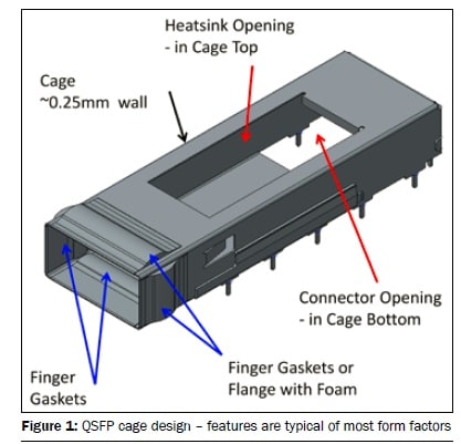
Pluggable optics modules, (POMs), such as SFP, QSFP, QSFP+, QSFP28, CFP, CFP2, and CFP4 transceivers, are optical interface devices that are connected to a PCB through ports in the faceplate. A brief description of these modules is given in Table 1. Initially conceived as low power devices, the module power density has increased along with demand for higher bandwidth. Consequently, it is progressively more difficult to cool these modules. The modules are hot-pluggable and the faceplate port utilizes a PCB-mounted cage. These cages are folded sheet metal enclosures that press fit into the PCB and provide connector alignment and electromagnetic compatibility (EMC) features as shown in Figure 1. The cages generally prevent heatsinking to module bottom but provide an opening in the top surface where a spring-loaded riding heatsink can contact the lid. The challenge is to permit the required sliding while providing a low interface thermal resistance.
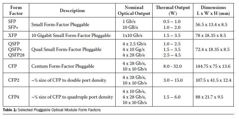
POMs are designed to support various communication standards. Multi-Source Agreements (MSAs) specify physical form factor and electrical interfaces. These agreements allow multiple manufacturers to make physically compatible products to promote competition, interoperability and multiple sources for systems vendors and end users. These MSAs become de facto standards. They also define power classes for POMs that are based on the supplied power and correspond to different internal processing levels and optical signal reach. POM data rates range from ~1 Gb/s to 100 Gb/s with a number of data rates available in each form factor. References [1] and [2] give physical dimensions of various form factors.
MSAs define the geometry of these optical modules, but parameters affecting the interface between a pluggable module and its heatsink have not been sufficiently well-defined or controlled. Some MSAs specify allowable contact forces, some do not. The surface finish and flatness of the module-heatsink contact area were recognized as requiring control, but limits were primarily set for low cost manufacturing methods and aesthetics. Initially some MSAs defined heatsinks, but due to the uniqueness of each system environment, system designers usually customized the designs. Increased module dissipation and functionality made it obvious that better thermal specifications were required.
This was recognized by the Optical Internetworking Forum, OIF, [3] who developed an Implementation Agreement (IA) [1] to specify general requirements for the thermal interface. The IA specifies that the MSAs [6, 8, 9 and 10] define the location and size of the contact areas where the majority of heat would be removed from high power modules and directly addresses the issue of removing heat from the top of the POMs. The IA defines resistance parameters of the interface between module and heatsink and specifies relevant information. It specifies the information POM suppliers must provide to facilitate thermal integration of the module within the host system for both the initial assessment and detailed design stages. These include specifications for temperature drop and thermal resistance between the module and an “ideal” heatsink. It defines a thermal interface resistance that includes interface contact and spreading effects. The IA recommends tighter tolerances for surface finish and flatness for well controlled interfaces. It defines power density classes for the thermal interface and describes a method for measuring the thermal interface resistance between the module and a cold plate with an “ideal” mating surface. In part 2 of the paper it’s appropriateness for the calibration of internal sensors used for module thermal alarms is discussed.
2. The Thermal Environment
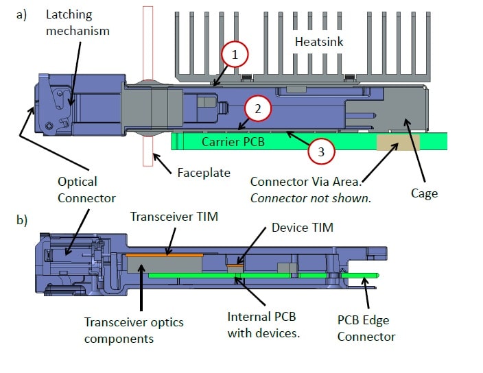
Pluggable optics modules combine fibre optic transmitters and receivers (transceivers) and some signal processing into one package. The transmitter side converts an electrical signal into light for transmission over optical fibre while the receiver section converts the light signal into an electrical signal. The modules plug into connectors on the host board for additional signal processing, switching etc. For all but CFPs, the modules are housed in a cage which guides the modules to the connectors and contains EMC solutions for the faceplate ports. The larger CFP modules use guide rails for alignment and have separate faceplate EMC features. The modules extend through the faceplate, and can be hot swapped. Figures 1 and 2 show typical thermally-important features of POMs.
Figure 2: a) QSFP in cage section at inside edge of cage, b) QSFP section showing typical internal layout. Narrow air gaps locations: 1) Module to top of cage, 2) Module to bottom of cage, 3) Bottom of cage to PCB, and not shown 4) sides of module to sides of cage.
The air gaps, ~0.2mm to 0.3mm nominal, between the module case and the cage, and between the cage and PCB provide an inconsistent thermal resistance because the tolerances and misalignments associated with manufacture and assembly are significant relative to the gaps. This precludes design using conduction to the PCB as a reliable method of cooling. In comparison, the electrical connection to the host PCB provides a well-defined thermal connection that can transfer heat into the module from neighbouring heat sources, or out to the PCB if it is relatively cool.
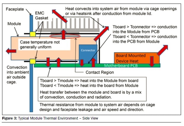
Figure 3 depicts the ways that heat is transferred between the module and the system. The relative merits of side-to-side or front-to back airflow are discussed in [2] where system and heatsink strategies for POM cooling are examined. A smaller amount of heat naturally convects from the module to the environment outside the faceplate. The thermal designer may have some influence on layout to prevent heating of the PCB near the connector. As noted in [2], in side-to-side air flow, cooling air arriving at the module and its heatsink is often much hotter than ambient, particularly for downstream modules in a densely filled faceplate.
For low power POMs on a cool PCB, a cage perforated with holes and conduction to PCB through the connector may be adequate for cooling. In this paper we are dealing with cases that require a heatsink. As illustrated in [2], there are several aspects to the heatsink design: the fin side, the base spreading, and the contact resistance between the module and the heatsink. The last two of these requires input and co-ordination between the system designers and the module suppliers/designers and is the focus of [1].
3. Flatness and Module Layout Studies on CFP2
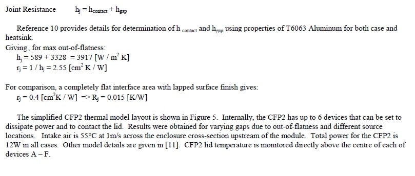
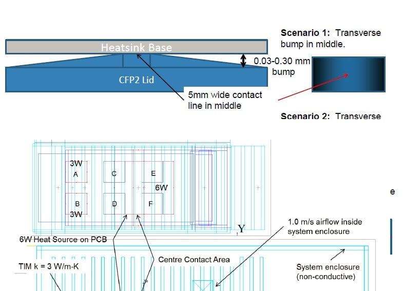
The initial work done in support of IA# OIF-Thermal-01.0 IA included a study of the thermal interface resistance between a CFP2 lid and heatsink base including heat spreading effects. The study examined three contact scenarios: 1) a transverse bump in the center of the lid, 2) a transverse hollow in the center of the lid and 3) a transverse contact in the center and ends of the lid. The stylized net-flatness-shapes of the three scenarios were used to bound the problem and are based on the authors’ module and heatsink surface measurements. All three scenarios were defined to have the same contact area. These simplified contact geometries are depicted in Figure 4 and the contact gap ranges from what would be an extremely fine production surface flatness to where both surfaces are out-of-flat by the maximum allowed by the MSA for the CFP2 contact surface. It was assumed for the study that both surfaces had the same type of out-of flatness so that modelling of the net gap between surfaces was easily implemented in the commercial CFD software [4] used for the analysis.
The resistance in the contact areas between the heatsink and the module was modelled using the method described by Yovanovich et al. [4]. Where:
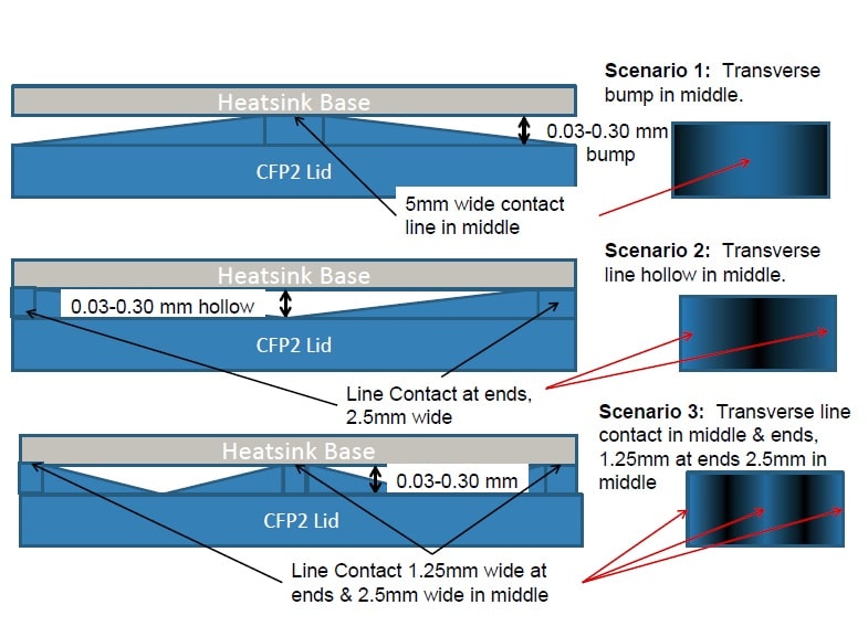
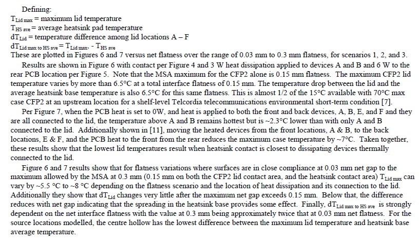
Figure 5: CFP2 flatness model layout showing front device, rear CFP2 PCB heat and central contact location
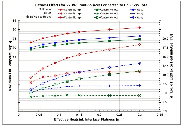
Figure 6: Range of flatness results with front device, and rear PCB heat dissipation
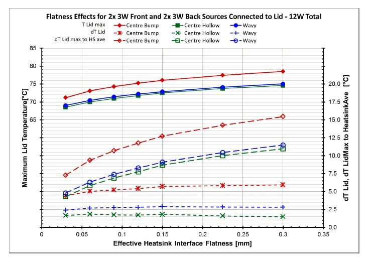
Figure 7: Range of flatness results with heat dissipation on front and rear devices with 0W PCB dissipation
4. Summary
Thermal interface resistance of a pluggable optics module is affected by design factors under the control of both the system designer and the module designer. In particular, surface finish and flatness have a strong influence within normally accepted manufacturing and machining practices.
Part 2 of this paper will examine the effects of increasing the thermal conductivity of the case as well as the effects of host PCB heat sources. It will also look at how to calibrate POM internal sensors.
References
1. IA# OIF-Thermal-01.0, Implementation Agreement for Thermal Interface Specification for Pluggable Optics Modules, Optical Internetworking Forum, May 18, 2015
2. OIF-PLUG-Thermal-01.0, Thermal Management at the Faceplate White Paper, Optical Internetworking Forum, March 2012
3. OIF website location: www.oiforum.com
4 Flotherm® V10.1 Computational Fluid Dynamics Software for Electronics Cooling by Mentor Graphics Corporation.
5. Yovanovitch, M.M., Culham, J.R., and Teerstra, P., Calculating Interface Resistance, Electronics Cooling, Article 3, May 1997, https://electronics-cooling.com/Resources/EC_Articles/May97/article3.htm
6. Hiramoto, K. Hardware Technical Editor, CFP MSA CFP2 Hardware Specification, Revision 1.0, July 2013, www.cfp-msa.org
7. TelcordiaTechnologies Generic Requirements, Generic Requirements for Telecommunications Data Center Equipment and Spaces, GR-3160-CORE, Issue 2, July 2013
8. Oomori, H. Hardware Technical Editor, CFP MSA CFP4 Hardware Specification, Revision 1.0, August, 2014, www.cfp-msa.org
9. SFF Committee, SFF-8663 Specification for QSFP+ 28 Gb/s Cage (Style A), Rev 1.5 April 2014, ftp://ftp.seagate.com/sff
10. SFF Committee, SFF-8661 Specification for QSFP+ 28 Gb/s 4x Pluggable Module, Revision 2.0, February 2014, ftp://ftp.seagate.com/sff
11. Mack, B., Graham, T., Thermal Specifications for Pluggable Optics Modules, 32 IEEE SEMI-THERM Symposium, March 2016.

