Due to the flexible manufacturing processes for producing BGA packages, there has been an explosion of new package designs, many of which contain more than one integrated circuit chip [1]. Existing industry standards for IC package thermal characterization apply only to single-chip packages. This Calculation Corner will present some techniques for calculating the junction temperature of a multi-chip module (MCM).
Existing JEDEC standards all assume that there is one heat source in a package, characterized by a single junction temperature, TJ [2]. This allows the use of thermal metrics that can be employed in calculations in a manner analogous to electrical resistors and that can be easily extracted from thermal measurements. The format of such a metric is
 |
where TREF is a reference temperature, measured in a specified location in a JEDEC-standard test environment, and P is the total dissipated power in the chip. Examples of reference temperatures are those of the ambient air, the test board, and the package case.
Clearly, this methodology breaks down when dealing with an MCM. First, it only accounts for a single junction temperature. Second, even when the power applied to one chip is zero, TJ,REF can be non-zero due to power applied to another chip in the package. Applying Equation 1 to the non-powered chip would involve dividing a finite value of
TJ,REF by zero power. This would lead to a value of infinity for
J,REF – not a very useful result.Intuition tells us that the temperature of any chip in an MCM would be affected by the particular combination of power levels applied to all the chips. This, clearly, represents a much more complicated situation than encountered with single-chip packages. The following discussion deals with two basic types of MCMs and provides some relatively simple means of dealing with them.
Basic Approach to MCM Analysis
Figure 1a and 1b illustrate two limiting cases of MCM design. The first is described here (for lack of a better term) as a “lateral” configuration. Each chip attaches directly to the substrate. Figure 1b illustrates the so-called “stacked ” configuration. (Of course, a given package could represent a combination of these configurations).

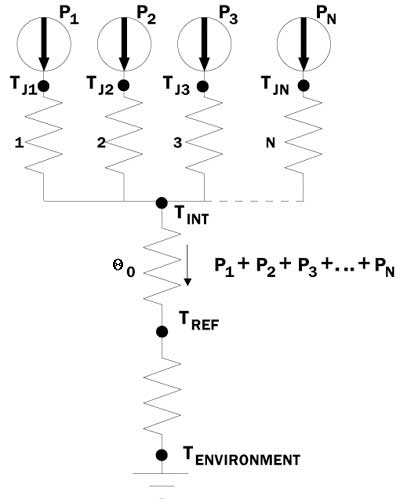
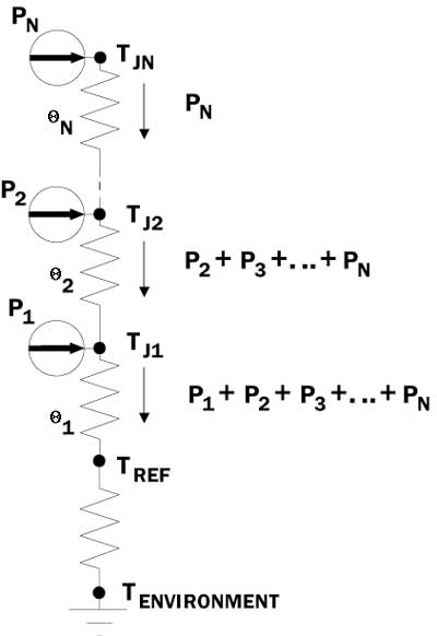
The thermal resistor networks in Figures 2 and 3 apply, respectively, to the two MCM configurations above, when they are tested in an industry-standard environment. TREF would be defined as in the existing JEDEC standards.
 |
Figure 2. Thermal resistor network for lateral-chip MCM.
 |
Figure 3. Thermal resistor network for stacked-chip MCM.In these Figures, TJi and Pi are the junction temperature and power, respectively, of the ith chip. i is the thermal resistance between the ith chip and adjacent downstream node in the network. The total number of chips is assumed to be N.In dealing with MCMs one must abandon the simple lumped resistor metric of the single chip package and deal with the actual temperature differences between each chip and TREF , while specifying the power levels applied to all the chips. This is expressed symbolically as
The actual function relating TJi,REF to the chip power levels will depend upon the MCM configuration.
Lateral MCM Configuration
The resistor network in Figure 2 applies to lateral configuration. The assumption is that the heat from the various chips will flow along parallel paths, until the heat flux converges to a region internal to the package, with a characteristic temperature, TINT. From there the heat will flow to the reference location and then to the environment. The following equation provides a solution to the resistor network for calculating the temperature of the ith chip.
 |
The accuracy of Equation 3 in describing the package thermal behavior will depend upon the extent that the region of mixing is a heat spreader with a nearly isothermal temperature. Even in situations in which this is not strictly true, Equation 3 is a useful approximation.
Stacked MCM Configuration
Figure 3 depicts a resistor network representing the stacked configuration. In this case the heat flow follows a series circuit. The heat flow through a given chip is equal to the power dissipated in that chip plus that of all the chips located above it. The temperature of that chip is equal to TREF plus the temperature difference at each chip location between it and the reference temperature. Note that the temperature of a given chip is not influenced by the temperature of a chip above it, only by its power. The following equations represent these concepts mathematically.
 |
Here again, these equations are only approximate for most packages due to the existence of paths for heat to flow to the reference region, which bypass the stack of chips. However, they are sufficiently accurate to be very useful in many situations.
Examples
The following examples make use of the preceding equations to estimate MCM chip temperatures when a JA value is known for an equivalent single-chip package. A JEDEC-standard test environment is assumed with the reference temperature equal to that of the ambient air. In these examples the temperature of the various chips is calculated using the appropriate formulas, above, and compared to the results of detailed finite element analysis (FEA) calculations. Certain details of the calculations are omitted due to space considerations. They are intended primarily to illustrate the calculation procedure and to provide an indication of the overall accuracy.
Lateral MCM Configuration
This example involves an MCM with a 4-layer substrate, containing 2 internal planes. Table I itemizes the various features of the package construction and operating conditions. There are 4 chips. Chip 1 is 6 x 6 mm. The other 3 chips are of the same size: 9.8 x 9.8 mm. 0.6 W is applied to chip 1. 1.0 W is applied to each of chips 2 – 4. The temperature, TINT, is assumed to be that of the upper plane. The method is as follows:
- Calculate an equivalent die size, based on the total chip area.
- Estimate
JA value for single-chip package, assuming this equivalent die size. (This value can be estimated from available test or simulation results).
- Calculate thermal resistance between this chip and the upper plane using a simple 1-D heat flow calculation based on the die area [3]. Call this
1, applying the notation of Figure 2 and Equation 3 to the single chip package (N = 1).
- Calculate
0 using Equation 3 (N = 1):
- Calculate
i for each of the 4 chips based on their individual areas using 1-D formulas.
- Calculate DTJi,AIR for each of the four chips using Equation 3.
The results of each step in the calculation are presented in Table 1. The calculated values of TJi,AIR is largest for chip 1, due to its small size. This quantity is the same for chips 2 – 4, indicative of their identical size and power level. There is reasonable agreement between the results calculated here and those from FEA. In general, errors could be expected to be as large as 15%. Note that the FEA calculation shows the effect of the precise die position in that
TJi,AIR is not the same for each of chips 2 – 4.Table 1
|
||||||||||||||||||||||||||||||||||||||||||||||||||||||||||||||||||||||||||||||||||||||||||||||||||||||||||||||||||||||||||||||||||||
Stacked MCM Configuration
This example involves a typical stacked-chip MCM: a chip-scale package containing 2 dies. Its construction features are noted in Table 2. The dissipated power in each chip is assumed to be 0.6 W. As above, the procedure involves the use of an estimated value of JA and the appropriate formula, Equation 5, to calculate the temperature of each chip.Table 2
|
||||||||||||||||||||||||||||||||||||||||||||||||||||||||||||||||||||||||||||||||||||||||
The procedure is the following:
- Estimate
JA value for a single-chip package, assuming a die size equal to that of the bottom die.
- Calculate
1 using Equation 5 (N = 1):
1 =
TJ1,REF/PTOTAL =
JA. Assume that this same value of Q1 can be applied to the MCM (N = 2).
- Calculate
2 using 1-D formulas, based on the area of chip 2. Typically this would be the sum of the thermal resistances of chip 2 and its associated die attach layer.
- Calculate
TJi,AIR for each of the two chips using Equation 5.
Note that the value of TJi,AIR for chip 1 (the lower chip) in the MCM is much higher than in the single-chip case since the total power of both chips is flowing through it. The agreement between the simple calculation and FEA simulation is quite good. In general, however, errors of up to 15% should be expected.
Conclusions
Thermal characterization of MCMs involves the specification of temperature differences rather than the usual thermal metrics. JEDEC-standard test environments and reference temperatures developed for single chip packages apply also to MCMs. Relatively simple formulas can be applied to estimate chip temperatures in many MCM configurations.
Further Reading
More precise calculations of MCM thermal performance based on the Principal of Superposition may be found in references 4 and 5.
References
- B. Guenin, “The Many Flavors of Ball Grid Array Packages,” Electronics Cooling, Vol. 8., No. 1, February, 2002, pp. 32-40.
- All JEDEC thermal standards can be found at the JEDEC web site, www.jedec.org, in the following series: EIA/JESD51-X.
- B. Guenin, “1-Dimensional Heat Flow,” Electronics Cooling, Vol. 3., No. 3, September, 1997, p. 15.
- B. Lall, B. Guenin, and R. Molnar, “Methodology for Thermal Evaluation of Multichip Modules,” IEEE Trans. Comp., Packaging, Manuf. Technol. – Part A, Vol. 18, No. 4, December 1995, pp. 758-764.
- B. Zahn, “Steady State Thermal Characterization of Multiple Output Devices Using Linear Superposition Theory and a Non-Linear Matrix Multiplier,” Proceedings SEMI-THERM XIV Conference, March, 1998, pp. 39-46.


