The proliferation of digital cameras and their subsequent modular integration in mobile communication and hand-held devices has made today’s photography almost trivial. The latter, i.e., the integration in mobile and hand-held devices is largely made possible by advancements in imaging technology as well as miniaturizing optics and the requisite electronics.
Most camera modules in mobile phones are now a fraction of an inch in dimensions and their thicknesses are approaching those of chip packages. This costing and technology report on Samsung S7 phone states that the camera module with a set of 6 lenses, gyroscope and optical image stabilizer (OIS) driver with flash memory is only 12x12mm in size with a thickness of 5.3mm.
SLR (single lens reflex) cameras of yesterday are mostly mechanical and electromechanical devices requiring no thermal management during their operation. The material sets used in their manufacturing withstood the extremes of temperature and, for the most part, functioned as intended. However, this is not the same with digital cameras – both standalone SLRs and integrated camera modules. The main “light engines” in these devices largely fall into two broad categories: charged couple devices (CCDs) and CMOS imagers.
An excellent introduction to the digital camera technology can be found in this article which succinctly defines all of the underlying terms and technology of image capture with the two broad categories of sensors and their variants. CCDs and CMOS imagers each have their distinct advantages and performance metrics. Their comparison makes sense only in the context of an application; this paper provides a good comparison between the two types of sensors. In general, CCDs produce superior image quality but are bulkier to package and cool.
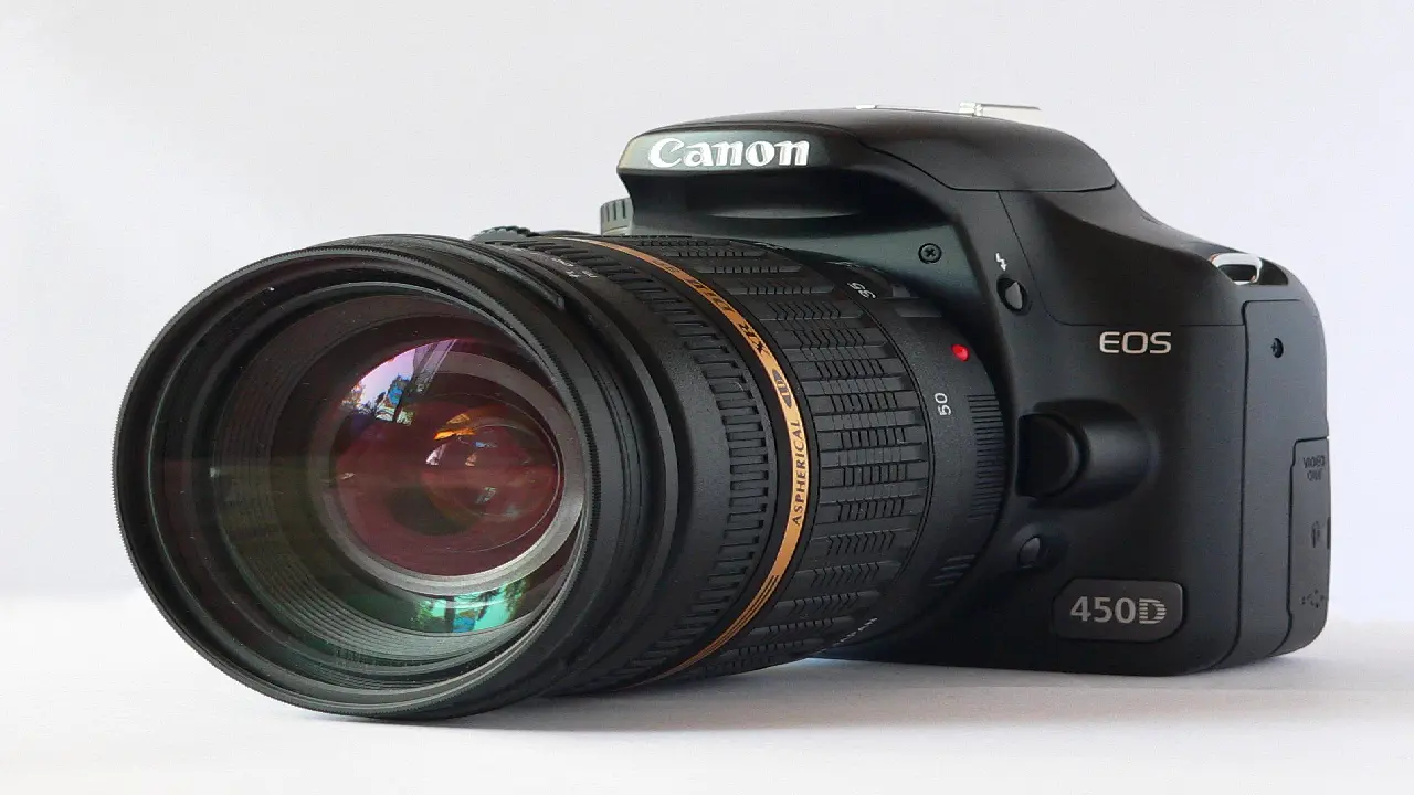
In an earlier article, I briefly covered the topic of dark currents in CCD imagers and the need for Thermoelectric (TE) modules to cool the CCD arrays minimizing dark currents. At lower temperatures of the CCD sensor, the ‘dark count’ pixels are lower. The CMOS sensors on the other hand are mostly uncooled, even in cases where the CMOS sensor array is a large one, like the Canon EOS 450D, which has a 12.2M pixel sensor measuring 22.2 x 14.8 mm.
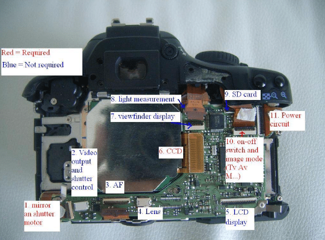
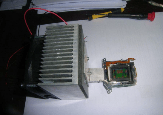
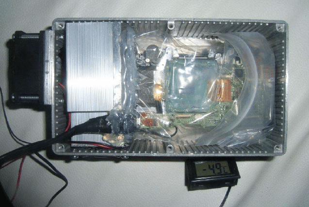
However, for astronomy imaging applications where the ‘dark count’ needs to be minimum, third party Peltier cooling adapters are available for most DSLR cameras. This hyper modification study details how one can disassemble the Canon 450D (XSi) Camera for cooling with heatsink augmentation.


For those of you who are hobbyists interested in building your own DSLR camera from scratch, there is an open source project that will be of interest. The “Build Your Own SLR Camera from Scratch” at SLR Lounge features an open source project for a SLR camera with full documentation and downloadable files. Some parts of the camera, including its body, can be 3D-printed. This project is perfect for designing a more elaborate cooling solution instead of a retrofit for the CMOS imager that can be perhaps integrated in the camera body. (Electronics Cooling would be very interested in hearing about your experience, perhaps in a blog. If interested, please contact me!)
In general, most digital cameras based on CMOS imagers are uncooled. The camera body is utilized as a heatsink with minimal compensation for dark currents in the imager. This has not stopped companies like Apple to get more creative in thermal management of consumer electronics devices. Apple patent “Multi-Level Thermal Management in an Electronic Device,” application #20120311357, 2012 is one such example.
In the coming weeks and months, Electronics Cooling will feature more articles on thermal management in Consumer Electronic Devices. Leave us a comment below!
by MP Divakar, PhD, Stack Design Automation
Technical Editor, Electronics Cooling


