Co-authored by: David L. Saums and Tim Jensen
DS&A LLC and Indium Corporation
INTRODUCTION
Electronic systems, implemented in such diverse industries as aerospace, vehicle, geothermal exploration, and mobile devices with a range of more challenging application conditions, create new challenges for component and material reliability. Non-flat mounting conditions, increases in ambient and operating temperatures, effects of moisture, corrosive gases, dust, and vibration can all affect product reliability, leading to the development of increasingly specialized categories such as thermal interface materials (TIMs).
FUNCTION
Not all thermal interface materials are alike or designed to perform under the same conditions. A single criterion, such as bulk thermal conductivity, is insufficient to assess overall performance and reliability. Attention to improving the selection and application of TIMs has gained in importance to improve overall assembly thermal resistance. An ideal interface (with perfectly polished and flat mating surfaces) would require no material between the two components; however, at a prohibitive cost. A TIM acts as an intermediate medium that eliminates the insulating layer of air that would otherwise be present in the interface. Maximizing thermal performance is a primary goal for the selection of a TIM; other factors include attributes that meet specific application needs, such as relative thixotropicity, ease of rework, ability to fill a stated gap, and durability.
An important factor for reducing thermal resistance of a TIM is minimization of the thickness of applied material, i.e. “bond line thickness”. Ideally, materials are as thin as possible, have no voids and are compressible under clamping that is used to ensure a thin bond line Many TIM contain a paste- or gel-like carrier and thermally conductive fillers. Paste or gel carriers improve the material’s contact for minute surface imperfections, i.e. “surface wetting”, but also can lead to separation or outgassing of the carrier under temperature. Reliability testing includes power and thermal cycling, humidity, extreme temperatures, dynamic loading, etc. Characteristics related to assembly processes for the material, such as working life, bond line thickness (post-assembly), dispensing process, rework, and environmental characteristics must be considered.
MECHANICAL CLAMPING AND THERMAL RESISTANCE
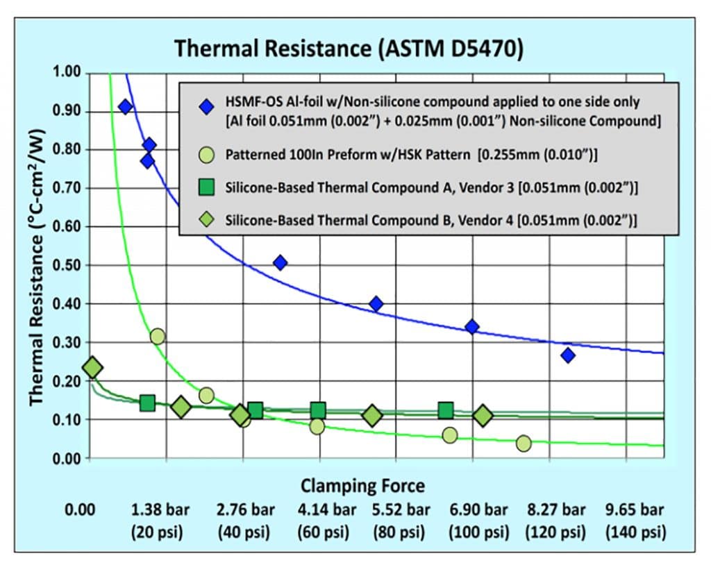
The ideal solution is application of the thinnest layer of TIM that is practical, with a high clamping force to ensure metal-to-metal contact in the high point areas and to force movement of the TIM to fill low points and microscopic surface imperfections, such as machining marks. The combination of applied force and the thinnest of materials are desirable, given the low bulk thermal conductivity of TIM organic compounds such as gels, thermal greases, and phase-change forms. The specific clamping force on an organic, thixotropic TIM, rather than its bulk thermal conductivity, primarily determines thermal resistance of the interface. Clamping force is also important for graphitic and metallic TIMs and is achieved with mechanical fasteners applied to the thermal solution. (No mechanical fasteners are required if a simple adhesive is sufficient.)
Figure 1 shows an example of how applied force affects thermal resistance of a TIM. Even though these solid materials do not include a surface-wetting carrier, clamping force plays a critical role and should not be ignored.
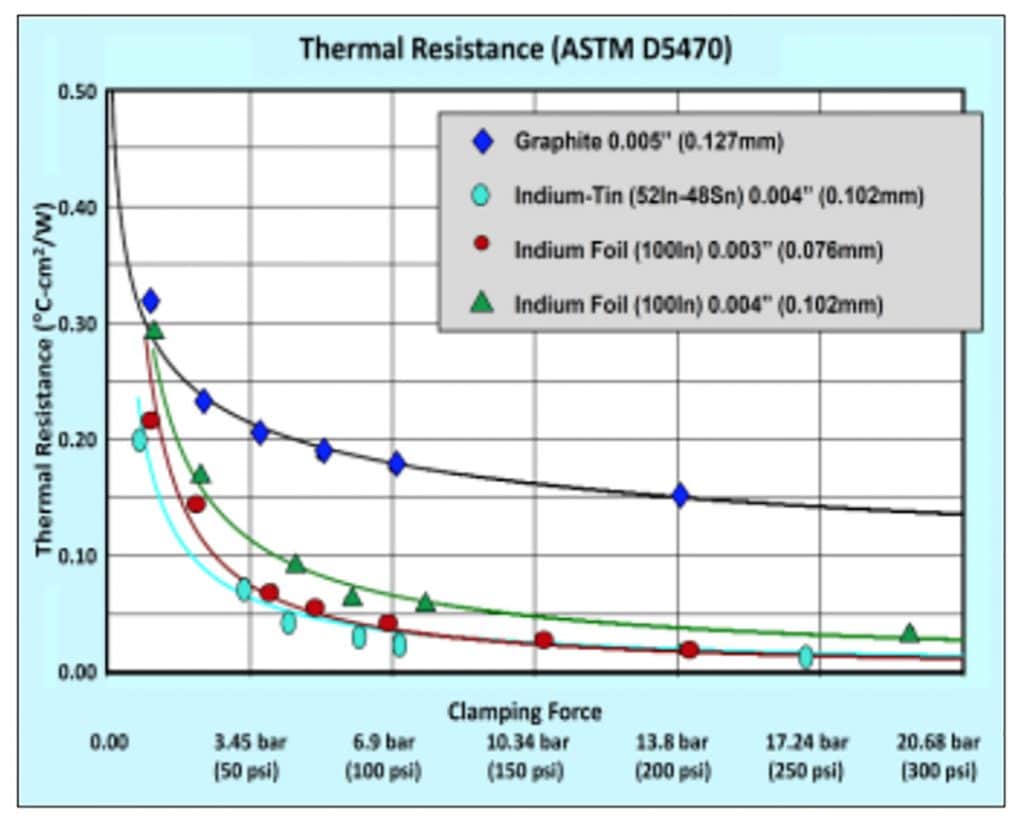
Testing of TIM materials for thermal resistance per unit area may be accomplished per an industry standard methodology, ASTM D 5470-12 [1]. The primary value of ASTM D 5470-12 as an accepted standard methodology is to allow direct comparison between data sheet values. Application-specific test vehicles and thermal test die may also be used [2, 3].
NON-FLAT CONDITIONS
Mounting surfaces need to be designed to be as close to parallel as possible, post-assembly. Increasing clamping force minimizes TIM thickness and improves thermal performance, and additional characteristics such as flatness, roughness, and co-planarity must be considered. Surface roughness and flatness criteria are typically called out in the manufacturing specification for a heat sink or cold plate mounting surface, and may be designated milled surfaces only in specified areas on a cold plate surface, to avoid milling an entire surface, to reduce cost.
The sum of the maximum out-of-flat specification for the module baseplate external surface and the maximum out-of-flat specification for the liquid cold plate can exceed 250 µm, in worst cases. For example, the largest IGBT modules (190mm) may have a total gap of 50-270 µm while smaller modules, such as the Infineon EconoDUAL™, may exhibit a total gap value of approximately 50 µm at locations, such as the center of the module [4].
TIM materials also need to address “non-flat” conditions that may be due to die warpage in ICs or purposeful design approaches such as engineered domes, found in the largest IGBT power semiconductor modules that utilize AlSiC (aluminum-siliconcarbide metal matrix cast composites) baseplates. A specific patterning of TIM application is called out in manufacturer specifications and torqueing sequences are identified to properly apply the necessary clamping load [5].
IGBT module assembly operations, such as soldering or sintering may create physical stresses within the baseplate of an IGBT module that can potentially lead to warpage; modules can dissipate significant power (kilowatt range) with heat fluxes that can be detrimental to ceramic substrates and other materials, due to thermal expansion coefficient mismatches. Operation of a large IGBT module with rapid switching, in applications such as traction and wind turbine converters, creates acute conditions for a TIM that can induce “pump-out” of greases and other organic compounds. Rigid materials, such as graphite and metallic TIMs, may degrade due to tearing if relatively brittle forms are selected.
Surface warpage may be present if the heat source contact surface is a silicon (or GaN or other) die in a non-lidded package configuration.
Semiconductor test and burn-in commonly have non-flat conditions by design. Test heads often have gimbaled mounts to allow slight rotation for devices with different footprints. Semiconductor burn-in (temperature cycles to 145-185°C) may require thousands of contacts with a single TIM. These factors, combined, severely limit options for TIM selection.
HARSH ENVIRONMENTAL CONDITIONS
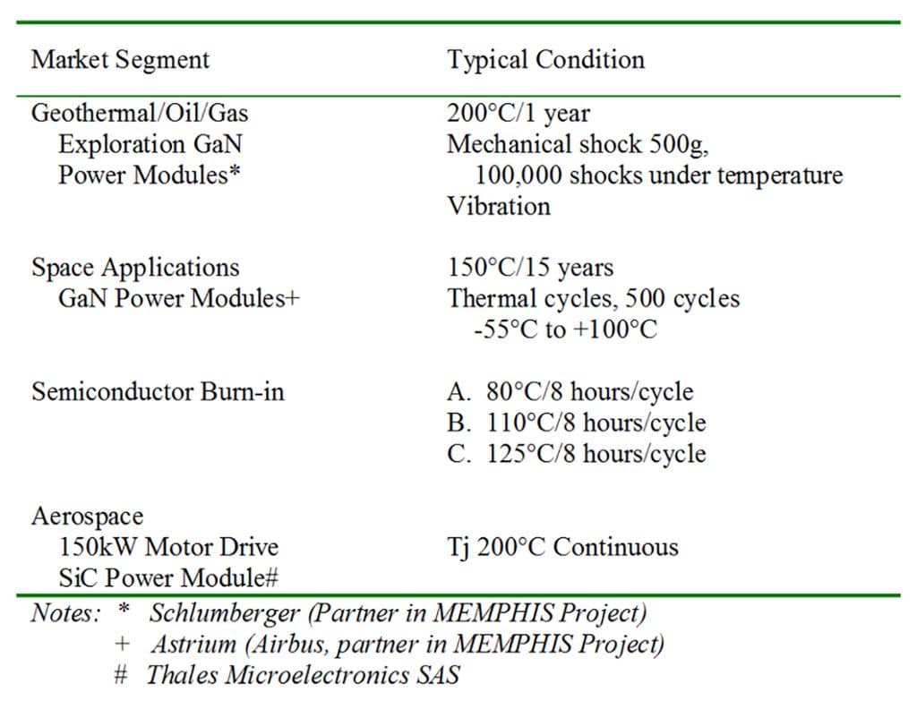
Increasingly specialized TIM development is also driven by increasingly harsh environmental conditions, and may be combined with non-flat conditions. Monitoring tools for geothermal/oil/gas exploration, as an example, include temperatures (and shock, vibration, and corrosive gases) well above typical automotive underhood values, generally beginning at 225°C. Table 2 provides examples in selected industry market segments [6, 7, 8].
Metal and graphite sheet TIMs provide the high durability and thermal conductivity desirable for high clamping forces and nonflat surface conditions. They also provide the critical benefit of meeting residue- and outgassing-free application requirements. Higher cost of metallic TIMs can be offset with reclamation programs. Absence of a silicone oil carrier is critical in systems with optical, optoelectronic, and diode laser components in which outgassed silicone may redeposit on lens elements and electrical contacts. While the avoidance of silicone redeposition is not typically considered under the umbrella of harsh environment requirements, this is a specification that is increasingly found in individual system OEM requirement statements.
RECENT TIM DEVELOPMENTS FOR NON-FLAT CONDITIONS
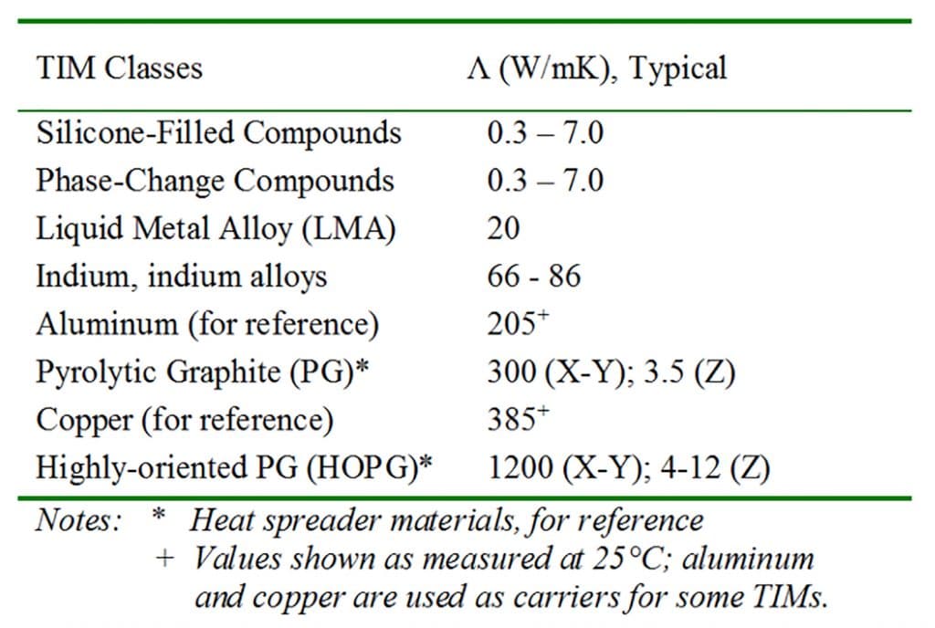
A very wide range of TIM relative bulk thermal conductivities can be found; Table 3 shows values for common as well as more recently developed materials. Note that certain materials shown have properties that are important differentiators between conventional TIM and heat spreader materials, a different material category with different requirements.
Recent TIM development programs include graphite sheet materials, primarily used for in-plane heat spreading with relatively little through-plane heat transfer. These materials are inaccurately referred as TIMs, largely because the materials are generally somewhat similar to TIMs and vendors are commonly TIM manufacturers [10, 11, 12].
Related recent TIM developments use vertically-aligned graphite fiber and carbon nanotubes; several commercialization efforts are vertically-aligned CNTs (“VA-CNT”) in polymeric carriers [13]. Vertically-aligned carbon fibers (“VA-CNF”) with polymeric carriers have been commercialized; one form of VA-CNF has been developed with a single-sided construction for the semiconductor test and burn-in market requirements [14, 15].
RECENT METALLIC TIM DEVELOPMENTS FOR NON-FLAT AND HARSH ENVIRONMENT CONDITIONS
Metallic TIMs have been used in die-cut preforms for decades in telecommunications, radar, and other flange-mount RF semiconductor markets. Additionally, reflowed indium solders in “TIM1” (between the backside of the die and the underside of a lid, in a lidded IC package) have been a standard for major processor manufacturers since 2003.
Indium metal and related alloys are easily die-cut as a soft, compliant TIM with die-cut through-holes and other features. Patterning creates metallic TIMs that are expanded in different heights with different pattern formats for extreme gaps. Further developments in this area include the use of tin and other metals as well as aluminum cladding on one surface [16]. These are used for the largest-footprint IGBT modules, semiconductor test, enterprise server processor modules, and GaN RF devices [17]. These materials are particularly advantageous with large (190mm) IGBT modules in which a relatively large gap may exist; due to long-term reliability requirements, the mechanical pump-out, outgassing, or dry-out that can occur with silicone oil carriers must be avoided. Electrical conductivity of the TIM for GaN RF devices can be critical in applications such as phased-array radar [18, 19].
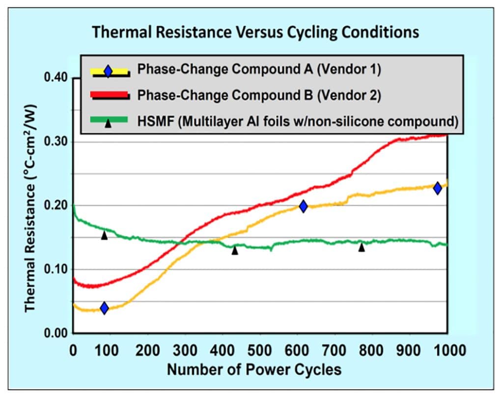
Another development in metallic TIMs is the application of siliconefree thermal compounds applied to one surface of an aluminum foil, targeted for semiconductor testing requirements where durability for thousands of contact cycles is needed. The surface without compound faces the Device under Test (DUT) to provide a durable contact without marking or residue [20]. For large gaps, two-layer aluminum foil coated with a non-silicone compound has been developed with total TIM thickness up to 250µm (0.0098”). Evaluation in electrical drives has been completed, including reliability testing in vertical orientations at elevated temperatures and high clamping force applied (1 to 15 bar).
Reliability testing of these expanded metallic TIMs has included power cycling to compare their performance to conventional TIMs, as shown in Figure 2.
Exceptionally high operating temperatures, such as those shown in Table 2, can limit options for TIM selection. Specialized metal TIMs manufactured with tin, lead, and copper have been developed for operating temperatures for higher temperature ranges [21].
SUMMARY
Specialized application requirements drive development of equally-specialized TIMs, including large area surfaces with large gaps, manufactured with different compositions and formats and now available for evaluation, particularly for use in environments not suitable for conventional TIMs.
ACKNOWLEDGMENTS
Contributions made to these development programs with dozens of thermal resistance, thermal cycling, and power cycling tests by Bob Jarrett, with support from Carol Gowans, Seth Homer, and Ron Hunadi, of Indium Corporation.
REFERENCES
- ASTM International, ASTM D5470-12, Standard test method for thermal transmission properties of thin thermally conductive solid electrical insulation materials, ASTM International, Philadelphia PA USA, 2012.
- C. Lasance, C.T. Murray, D.L. Saums, M. Renz, “Challenges in Thermal Interface Material Testing,” Proceedings, Semitherm Symposium 22, Dallas TX USA, March 13-15, 2006.
- R.N. Jarrett et al., “Comparison of Test Methods for High Performance Thermal Interface Materials,” Proceedings, Semitherm Symposium 23, San Jose CA USA, March 2007.
- Infineon Technologies, “EconoDual™3 Automotive Qualified,” www.infineon.com; and “Product Brief B133H9384-V7-7600-EU-EC-P, EconoDUAL™, EconoPACK™ 4, EconoPACK™ + Product Family,” describing the Econo medium voltage IGBT module products.
- Fuji Electric PrimePack Mounting Instructions (11/2014): https://www.fujielectric.com/products/semiconductor/ model/igbt/mounting/box/doc/pdf/MT_IGBT/ MT5Q01780_E.pdf
- M. Massiott, W. Serrano, “MEMPHIS Project Overview and High Temperature Packaging Development,” IMAPS France 8th European Micropackaging and Thermal Management Workshop, La Rochelle, France, February 2013.
- Thales Microelectronics SAS, Data sheet, “Harsh Environment Power Inverter, ” 2015.
- K. Stentoft, M.L. Petersen, “Electronics in Harsh Environments – Product Verification and Validation,” IEEE Reliability and Maintainability Symposium 2008, Las Vegas NV USA, January 28-31, 2008.
- DS&A LLC (Multiple sources).
- M. Getz, M. Smalc, “New Developments in Flexible Graphite Thermal Interface Materials,” IMAPS Advanced Technology Workshop on Thermal Management 2013, Los Gatos CA USA, November 5-7, 2013.
- R. Prieto, J.P. Colonna, P. Coudrain, C. Santos, P. Vivet, S. Cheramy, D. Campos, A. Farcy, Y. Avenas, “Thermal Measurements on Flip-chipped System-on-Chip Packages with Heat Spreader Integration,” Proceedings, Semitherm Symposium 30, San Jose CA, March 2014.
- D. Saums, “Developments in Advanced Thermal Materials,” IMAPS France 10th European Micropackaging and Thermal Management Workshop, La Rochelle, France, February 2015.
- H. Taphouse, B. A. Cola, “Thermal Expansion in Carbon Nanotube Forest Interfaces,” Proceedings, IMAPS Advanced Technology Workshop on Thermal Management, Los Gatos CA USA, November 2013.
- R. Yamamoto, “Thermal Interface Material with Controlling Graphite to Orient Vertically,” IMAPS Advanced Technology Workshop on Thermal Management, Los Gatos CA USA, November 12-14, 2012.
- I. Sauciuc, et al., “Carbon Based Thermal Interface Material for High Performance Cooling,” Electronics Cooling Magazine, December 2014.
- G. Wilson, “Sn+ Metallic Thermal Interface Materials for Superior Thermal Management,” Proceedings, IMAPS France 10th European Micropackaging and Thermal Management Workshop, La Rochelle, France, February 2015.
- Z. Radivojevic, K. Andersson, L. Bogod, M. Mahalingam, J. Rantala, J. Wright,; “Novel Materials for Improved Quality of RF-PA in Base Station Applications,” IEEE Transactions on Components and Packaging Technologies, vol. 28, no. 4, pp 644-649, December 2005.
- Z. Radivojevic, K. Andersson, J.A. Bielen, P.J.V.D. Well, J. Rantala, “Operating Limits for RF Power Amplifiers at High Junction Temperatures,” Microelectron. Reliability, vol. 44, pp. 963-972, 2004.
- T. Jensen, D. Saums, “Metallic TIM Testing and Selection for Harsh Environment Applications for GaN RF Semiconductors,” IEEE Phased Array System Technology Conference, Waltham MA USA, October 17-21, 2016.
- J.A. Sanchez, “Challenges of Thermal Interface Materials in Test of IC Packages,” IMAPS Advanced Technology Workshop on Thermal Management 2013, Los Gatos CA USA, November 5-7, 2013.
- D. Saums, T. Jensen, “Development, Testing, and Application of Metallic TIMs for Harsh Environments and Non-Flat Surfaces,” IEEE I-THERM Conference 2017, Orlando FL USA, May 30-June 2, 2017.

