Bruce Guenin, Assoc. Technical Editor
Introduction
As integrated circuit (IC) devices get more complex, the interconnections between them provided by printed circuit boards (PCBs) get more complicated as well. Thermal simulation software tools are getting more capable of importing PCB layouts and automating the process of creating a model of the PCB whose local thermal conductivity is representative of the underlying layout. However, in many cases, it is necessary to perform a thermal model of a package on a PCB without creating a highly detailed model of a PCB. This article is the first of a series of columns that will explore the effectiveness of different strategies for accurately accounting for heat transfer into a PCB while using a simplified solid model of the PCB.
Thermal Model
The heat generated by an IC often has several flow paths into the PCB it is mounted to. Quite often in a ball grid array (BGA) packages the central balls connect to vias in the PCB that route the heat directly into the power and ground planes in the PCB. In contrast, the peripheral balls tend to be connected to surface traces on the PCB. Some of the heat conducted by the traces flows directly into the ambient air. However, most of it will flow to the interior of the PCB and enter the power and ground planes. These planes are typically effective in spreading the heat from a given package over a large area in the PCB, whence it can flow more efficiently into the ambient air.
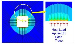
Figure 1a) Temperature contour map, top surface of board
This analysis is devoted to exploring the heat transfer from the traces to the inner planes of the PCB. Any other heat flow path into the PCB is neglected in the model. The construction of the model is illustrated in Figure 1. The portion of the PCB where a package would normally be mounted has been removed. This exposes the cross-section of each of the traces at the periphery of the cutout. Heat flux is applied to the exposed surface of each trace. The magnitude of the heat flux to chosen so that a total of 1 W of heat is injected collectively into all of the trace cross-sections. There are adiabatic boundary conditions at the exposed cross-section for each trace so that all the applied heat flows from that surface into the trace.
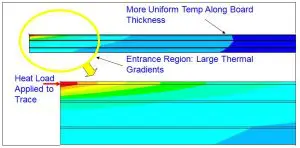
Figure 1b) Temperature contour map along cut through centerline. Both figures illustrate the method used of applying a heat load directly to the exposed cross-sections of the traces at the periphery of the cutout [Ref 2].
For convenience, the PCB geometry corresponds to that of a JEDEC-standard PCB, that would be used in the thermal testing of BGA packages [1]. The board consists of six layers: the top metal traces, two interior planes, and three dielectric layers. The board is 101 mm sq. and is 1.54 mm thick. The interior planes are 35 µm thick. For reasons of test reproducibility, the traces on a JEDEC-standard PCB are 70 µm. However, in PCBs used in products, a 35 µm thickness is more common. Traces of both of these thickness values are analyzed in the model. The cutout in the PCB is 27 mm sq. Further details regarding the PCB construction may be found in a previous column [2].
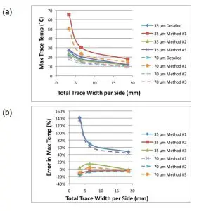
Figure 2- Graphs depicting simulation results from Table 2 versus total trace width per side of the cutout in the parallel region of the traces: a) maximum trace temperature and b) error in maximum trace temperature.
A commercial finite element analysis (FEA) software tool was used to generate solid models of the multilayer board with a number of different trace configurations [3]. In all cases, the thermal solution was obtained assuming an ambient temperature of 0 ˚C (so that the reported temperatures represent T – TAmbient) and a heat transfer coefficient of 10W/m2K (typical of natural convection cooling) was applied to the top and bottom surfaces of the PCB.
The trace geometries are represented accurately in the model. Since the model was generated with an appropriately refined FEA mesh, the model results are assumed to be “exact” when compared with the results of the models having simplified geometries.
Table 1 presents the various parameters characterizing the trace geometries for the three configurations studied. Each configuration has an “a” version and a “b” version. In all of the “a” versions, the trace thickness is 35 µm. In all of the “b” versions, it is 70 µm.
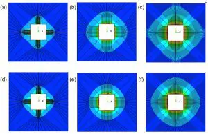
Figure 3 – Contour plots for three configurations (1a, 2a, and 3a) evaluated using two different methods (Detailed and #3) : a) Config 1a, detailed; b) Config 2a, detailed; c) Config 3a, detailed; d): Config 1a, Method #3; e) Config 2a, Method #3; f) Config 3a, Method #3.
The images in Figure 3 illustrate the trace pattern of each configuration. [Note that a discussion of the thermal contours in this figure follows later in this article.]
Simplifying Assumptions
It is common practice to represent the trace layer of a PCB as a continuous plane whose thickness equals that of the traces and whose thermal conductivity equals the copper coverage of the traces multiplied times the thermal conductivity of copper. This is commonly referred to as “smearing” the trace layer. This procedure is defined herein to be Method #1 and is specified as:
- Simplification Method #1: represent trace layers by a plane. Plane thickness = trace thickness. Plane effective thermal conductivity = Factor x thermal conductivity of copper. Factor = % of PCB surface occupied by the traces.
All of the simplified models discussed here represent the trace geometry by a plane. However, they differ by the method used to calculate an effective thermal conductivity of the plane.
The thermal contour maps in Figure 1 indicate a significant thermal gradient in the traces as heat flows through them on their journey into the internal planes in the board. The side view also illustrates that the heat flows from the traces to the top plane of the PCB in a gradual way, due to the relatively low thermal conductivity of the board FR-4 dielectric (0.25 W/mK). The flow of heat from the traces to the plane is affected by the fact that the traces do not represent a continuous plane. Hence the heat flows, not uniformly over the full area of the dielectric, but is concentrated in local regions, directly under each trace.
It should be noted also, that the temperature of the trace approximates that of the underlying plane after a distance equal to approximately 10 times the dielectric thickness. Hence, it is the portion of the traces near the package that make the most significant contribution to the heat flow between the traces and the top plane.
The insight gained by these observations leads to the formulation of two other methods of calculation of effective thermal conductivity values that represent a derating of the thermal performance of a smeared plane, that, otherwise, would provide a much more efficient thermal path to the top plane than do the individual traces.
- Simplification Method #2: represent trace layers by a plane. Plane thickness = trace thickness. Plane effective thermal conductivity = Factor x thermal conductivity of copper. Factor = % of PCB surface occupied by the traces near the package, where the traces are parallel.
- Simplification Method #3: represent trace layers by a plane. Plane thickness = trace thickness. Plane effective thermal conductivity = Factor x thermal conductivity of copper. Factor is calculated as in Method #2. The thermal conductivity of the dielectric between the inner plane and the top plane = Factor2 x thermal conductivity of the dielectric. Factor2 = trace width/trace pitch.
Calculated Results
The results of the calculations are detailed for all configurations in Table 2. The values of T,max for the 35 µm configurations are all higher than the corresponding ones for the 70 µm configurations, as expected. The values of T,max calculated using Method #1 are all higher than those calculated with the other methods. This should not be a surprise since Table 1 indicates that the % copper averaged over the entire PCB surface is much lower than that calculated for the parallel trace region. For example, for configuration 3a and 3b, the % copper averaged over the parallel region is 75%, whereas the % copper averaged over the entire PCB is only 16.7%.
Methods #2 and 3 yielded values of T,max that are much closer to the exact values.
The graphs in Figure 2 depict the relative behavior of the different methods. Both the actual values of T,max and % error are plotted versus a parameter = total trace width per side = trace width x number of leads per side. Higher amounts of copper lead to larger values of this parameter. The graphs show that the accuracy of Method #1 improves at the higher copper levels. However, even at high copper levels, the error is still over 40%. At the lowest copper levels evaluated here, the error for Method #1 exceeds 100%.
There is much better performance with Methods #2 and #3. Averaged over all the cases studied here, Method #2 had -9% error and Method #3, 1%.
Figure 3 depicts selected temperature contour plots for all three configurations, version “a” (35 µm traces). The top row of images shows the results for the detailed trace models. The lower row depicts the results in which Method #3 was applied to the calculation of the effective thermal conductivity of the plane and the top dielectric. The values of T,Max were similar for the two approaches for each case. However, the detailed trace models clearly show the impact of the trace routing on the thermal gradients. The contours for Method #3 show, in general, more of a circular symmetry. [Note that the apparent presence of the traces in the lower set of images depicting Method #3 results is an artifact of using the same finite element mesh for all the solution methods applied to a particular PCB configuration. However, in the Method #3 models (as well as for #1 and #2) the same material properties were applied to all elements in the trace layer, making that layer truly isotropic in its thermal behavior.]
It was mentioned earlier that the assumed heat transfer coefficient equaled 10 W/m2K, representative of natural convection. It should be noted that, for higher values of the heat transfer coefficient, the tendency for the heat to be transferred from the traces to the top plane in the region near the package would be even more pronounced. This would be expected to further increase the error in applying Method #1.
Conclusions
Three different strategies for using a convenient “smeared” planar layer to represent a layer of discrete traces were explored. The strategies that were most successful were based on an understanding of the local heat transfer between the traces and the top plane in the PCB that was presented in an earlier column [2]. They made use of the fact that most of the heat transfer between the traces and the top plane of the PCB occurs near the package and that the heat flow is concentrated in the vicinity of each trace and does not flow uniformly through the dielectric. Hence, the copper coverage near the package should be used in calculating the effective thermal conductivity of the smeared plane and the thermal conductivity of the dielectric should be derated by the same factor. The conventional method, which uses a value of copper coverage averaged over the surface of the PCB is much less accurate.
References
- See, for example: JEDEC Standard JESD51- 9, “Test Boards for Area Array Surface Mount Package Thermal Measurements,” available for free download at www.jedec.org.
- Guenin, “Entrance Effects for Heat Flow into a Multi-Layer Printed Circuit Board,” ElectronicsCooling, Vol. 10, No. 4, November 2004.
- ANSYSÒ, Version15.0.


