Introduction
Often new products or product concepts only introduce some new aspects and rely heavily on existing designs. At the board level this often means only one section of a board is retooled or upgraded; an approach that can save significant time and money. Unfortunately, we cannot rely solely on previous work because the interaction of old functions and new features often results in new design challenges. The new functional groups are often chosen to provide better performance or to introduce new technology, which typically means higher power dissipation. The higher power or lower temperature limits of new technologies increase the risk of causing thermal issues that may slow down the total design process.
Early and easy thermal assessment, which can now be completed in the stages before detailed routing, helps to alleviate potential problems. This allows thermal performance to be part of the design process as opposed to a validation and stop gap measure at the end of the design. This technical brief will demonstrate the advantages of thermal analysis early in the design of an updated board, and will discuss the thermal performance and potential design changes.
Example
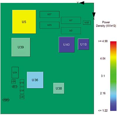
This application is based on the evolution of an add-on card measuring 6.5 x 5.5 in. (16.5 x 14 cm). The existing platform provides a uniform flow rate of 400 fpm at 35°C and the vertical heat sink volume is constrained by the 25 mm pitch between boards. In the original design, there is a high power density area in the top part of the board (Figure 1a and 1b). No thermal issues were identified with the original design during testing or validation. Based on the success of this product, a planned upgrade path called for new functionality requiring additional components.
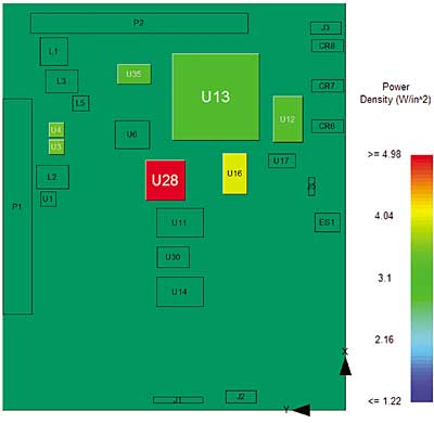 |
Figure 1a. Original board power density (top).
Figure 1b. Original board power density (bottom).
Concerned about the risks involved with the additional power and heat dissipation, the engineer can import the existing board (via IDF format) into a board-level thermal analysis tool from existing CAD models. Once the model is in the software, the engineer can strip out the constraints of the detailed design tools in order to explore various concepts quickly.
In this case, the signal integrity and routing requirements restrict the placement of new components to the upper section of the board around component U13. This increases the power density in the already populated area of the board (Figure 1c). Looking at this new design, we might expect some potential thermal issues, but the specific junction or case temperatures of these components are unknown at this time.
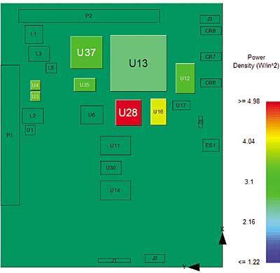 |
Figure 1c. New board power density (top).
The standardization efforts of JEDEC and the growing support of compact thermal models for analysis enable critical components to be modeled in more detail using 2-resistor or DELPHI models. Such models can be created with commercial thermal modeling packages or may be provided directly by the vendor. Both methods yield a component model that provides accurate junction and case temperatures traceable back to experimental validation. The remaining components are analyzed using solid models based on the detailed designs of the packages. All boundary conditions are combined, enabling the engineer to perform a full 3D CFD analysis and obtain component temperatures. The results shown in Figure 2a indicate that U37 and U28 exceed their maximum junction temperature of 90°C. The neighboring components not only affect the airflow, but also heat that section of the board, causing core component U13 to approach the specified maximum temperature. In some cases, exploring component placements can resolve this thermal saturation, but often electrical performance restricts the necessary displacement and relative positions are fixed.
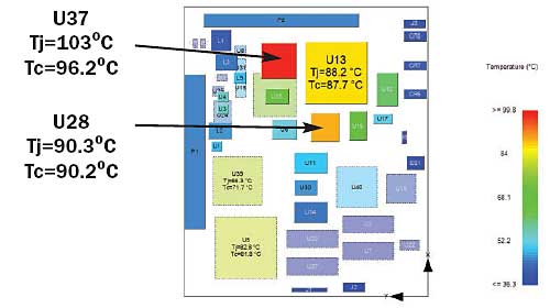 |
Figure 2a. Updated board temperatures.
Solutions
If the board placement is frozen, there are still several potential solutions, such as attaching a heat sink, adding thermal vias in the board below the components, or increasing the copper content locally to improve the heat spreading in the board. In this case, the option of transferring the heat into the board does not look like a viable solution. The next most cost-effective solution is the addition of heat sinks. In cost sensitive designs such as this, custom or exotic thermal solutions may kill the project. This makes it critical for an engineer to qualify a design early and to ensure that it can be adequately cooled with low cost heat sinks commercially available on the market. In an effort to reduce costs, the same 21 by 21 mm pin fin heat sink is placed on both U37 and U28. The thermal resistance between the component and the heat sink is reduced by introducing a thermal interface material. The results of the analysis including the heat sinks (Figure 2b) show that none of the components are above the junction temperature limit of 90°C.
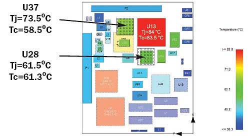 |
Figure 2b. Updated board with heat sinks temperature.
Overall, it is recommended to implement board thermal analysis as early as possible in the design cycle. This analysis will help highlight potential thermal issues and provide engineers with more flexibility in resolving them early, before hours of engineering time is invested in unusable designs. In addition to performing thermal analyses to optimize the thermal design of the board, it is desirable to perform simulations concurrently to evaluate the stress, reliability, and electromagnetic compatibility of the design until the physical prototype is built and tested to confirm the results found during the analysis.

