Toward A Thermal Figure Of Merit For Multi-Chip Packages
Bruce M. Guenin, Ph.D., Associate Editor
Introduction
Last issue’s Calculation Corner dealt with methods for predicting the temperature of each chip in a Multi-Chip Package (MCP) at an arbitrary combination of chip power levels using the
principle of superposition [1]. One of the main points of that article was that both the terminology for package characterization and the mathematical approach to device temperature prediction for an MCP are
different from that of a Single Chip Package (SCP). For an MCP the physics dictates that we speak in terms of the temperature difference between each device and a reference temperature at specified values of
electrical power supplied to the devices.
In the simpler SCP world, there is the luxury that the various thermal metrics in the form ΘJX are not only used for the prediction of the junction temperature in many situations. They also serve as performance figures of merit [2]. Generally,
ΘJX is the thermal resistance between the junction and a specified reference location (X). The JEDEC standard reference locations are: the ambient air (A), package case (C), or the printed circuit board (B). Of these, the most extensively used figure of merit for an SCP is
ΘJA. Even though it is not a good predictor of junction temperature in an actual application, it is extremely useful for comparing the thermal performance of different packages which exchange heat to
the ambient air by way of the printed circuit board to which they are attached. Of course, a smaller value of ΘJA is associated with higher performance.
This column will explore the utility of defining a performance figure of merit for an MCP inspired by the classic ΘJA for an SCP. It represents a snapshot of work in progress in the area of MCPs by the JEDEC JC15.1 Thermal Standards Subcommittee.
Thermal Figure of Merit for an MCP
The JEDEC standard for a thermal test chip to be used in a SCP specifies that it should generate a constant heat flux (power per unit area) over at least 85% of the
chip area [3]. It further specifies that the reported junction temperature should be that measured at the chip center, which, for a constant flux condition, would be the maximum temperature.
Standardized methodologies invariably involve a reduction of the options and permutations that exist in actual applications. This
simplification makes it easier for independent organizations working only from the standards documents to reproduce the required test conditions and sample configurations. Furthermore, it makes the job of
communicating the test conditions and results more efficient.
Even at the SCP level, the standard involves a simplification. Application chips normally have different functional blocks of circuitry that
generate different flux levels in actual use. Because of this, the maximum temperature in an application chip is usually not at the center. However, since the main purpose of the test is the measure the thermal
efficiency of the package, simplicity is gained by the constant flux requirement. Because of this requirement, only the overall chip size and total power need be specified.
This reasoning could be extended to MCPs. If a uniform flux is applied to each chip, then specifying the flux and x-y dimensions of each chip,
or equivalently, the total power and the chip dimensions will completely specify the power map. Simplicity would require that a single, equivalent junction temperature be calculated. An area-weighted average of the
temperatures for all the chips in the MCP is a reasonable way to proceed.
The figure of merit would, then, be calculated using the equation.
 |
where TJ,i and Ai are the junction temperature and area, respectively, of the ith chip, N is the total number of chips, and SRC=”http://s3.electronics-cooling.com/legacy_images/2006/11/phi_cap.gif” VSPACE=0 HSPACE=0 ALIGN=”TOP” border=0 ALT=””> is the flux, uniformly applied to all the chips.
The utility of this method is explored in the following sections by means of a thermal simulation.
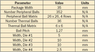
Table 1. Package Construction
 |
Thermal Simulation
A Finite Element Analysis (FEA) calculation was performed initially for a lateral four-chip MCP in a Ball Grid Array (BGA) package format attached to a JEDEC-standard test board.
This is the same configuration explored in the previous installment of this column [1]. Table 1 summarizes the principal geometrical parameters for the package.
This model was then modified to sequentially remove various chips to calculate the
chip temperatures in a three-chip MCP (chips # 1, 2, & 3) and then two configurations of a two-chip MCP (chips # 1 & 2 and 1 & 3). Furthermore a single chip equivalent package was
evaluated for each MCP configuration. The area of this single chip (assumed square) is chosen to equal the total chip area for the MCP equivalent packages.
The model was solved assuming a total power of 1 W applied as a uniform flux to the
top surfaces of all the chips in a given model. A constant heat transfer coefficient of 10 W/m2K was applied to all external surfaces of the package. The specific values of heat flux
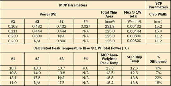
and power applied to each chip along with the calculated rise in the peak chip temperatures are presented in Table 2.
Table 2. Comparison of junction temp rise: MCP vs equivalent SCP
 |
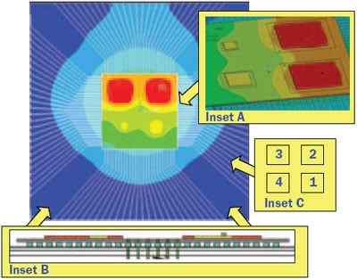
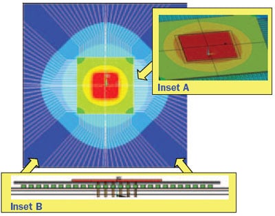
Figures 1 and 2 display the calculated temperature contours superimposed on the
solid model for the MCP and SCP configurations, respectively. In each case, an inset provides a side view of the solid model with the dielectric layers hidden to illustrate the
internal construction of the package and test board.
 |
Figure 1. Thermal simulation results for four-chip MCP attached to a JEDEC-standard test board. Insets
A and B show the model with dielectric layers hidden. Inset A: perspective view of chip locations. Inset B: side views showing metal layers and via structure in the package and board. Inset C provides
the numbering convention for the chips.
Since 1 W was chosen at the total power for each package, the calculated peak temperature for the SCP is equivalent to a ΘJA value. The smallest
ΘJA value (12.6 C/W) is for the largest chip (15.2 mm), having an area equivalent to all four chips. Conversely, the largest
value (13.8 C/W) is for the smallest chip (11.2 mm), with an area equal to that of the chips in the two-chip configuration.
 |
Figure 2. Thermal simulation results for an SCP attached to a JEDEC-standard test board.
Chip size = 15.2 mm.
For the various MCP configurations, the calculated value of the FOM increases with
a reduction in the number of chips and, equivalently, with the decrease in the total chip area. For the four-chip configuration, the value of the FOM is 6% greater than ΘJA for the
equivalent SCP. For the three-chip package it is 7% greater. Finally, for the two-chip MCP, it is either 18% or 22% greater, depending on the chip configuration.
This behavior can be explained entirely by noting the relative position between the
chips in the various packages and the centrally-located thermal-via/thermal-ball array, which serves as a preferential path for transmitting the heat from the chips to the upper plane in the
board. This plane plays an important role in cooling the chips by spreading the heat beyond the package outline over the full surface of the board thereby improving the transfer of heat to the ambient air.
In the SCP, heat flows to the thermal via array directly from the bottom of the chip.
Very little heat spreading is involved. From the largest to the smallest chip in the SCP, the same heat transfer area is offered to the chip by the thermal via array.
This should be contrasted with the MCP configuration, in which none of the chips
directly overlap the thermal via array. For these chips, heat must first spread through the metal planes in the laminate before reaching the array. This process is moderately efficient
for the four- and three-chip MCP configurations, since the major heat flow to the array, from the two 10 mm chips, occupies two quadrants of the planes. However, in the two-chip
configuration, most of the heat is generated in a single 10 mm chip, which utilizes roughly a quadrant of the metal plane in transmitting the heat to the array. This leads to a considerable
falloff in package performance.
It is interesting to note that by doing this sort of performance comparison between an
MCP and an equivalent SCP, a performance shortfall can be identified. It may also lead to identifying an appropriate corrective action in the design of the MCP. For example, an
obvious remedy would be to position directly under each chip a dedicated thermal via/thermal ball array to route the heat to the top plane of the board.
Conclusions
The preceding analysis suggests that the proposed FOM can be used in much the same way for an MCP as the more familiar ΘJA in evaluating the performance of an SCP.
There are, of course, tradeoffs with this method. In effect, it treats all the chips in an
MCP as if they were of equal importance from a thermal point of view. This is not true in a typical MCP. The chips that have higher flux levels, a lower maximum junction temperature,
or some combination of the two, require special attention in determining whether a particular package design is adequate for a given application.
However, even in the face of such subtleties, a simple, consistent thermal figure of
merit could be a reasonable starting point in determining the suitability of an MCP design.
As the JC15.1 Subcommittee proceeds in its standardization efforts for MCPs, one of
its challenges will be finding the right balance between simplicity and generality, on the one hand, and relevance to particular applications on the other. The process will almost inevitably
lead to changes to the method suggested here. It is hoped that this article will generate discussions regarding these tradeoffs and ultimately lead to a better standard.
References


