Advances in microfabrication processes have led to a continuous miniaturization of Field Effect Transistors (FET) that contain semiconductor (e.g., silicon), insulator (e.g., silicon dioxide), and metallic (e.g., copper interconnects) layers only a few nanometers thick. Ever increasing demand for faster microprocessors and the continuous trend to pack more transistors on a single chip have resulted in an unprecedented level of power dissipation, and therefore higher temperatures at the chip level. Thermal phenomena are not directly responsible for the electrical functionality and performance of semiconductor devices, but adversely affect their reliability.
Three major thermally-induced reliability concerns for transistors are failure due to the electrostatic discharge phenomenon, stresses due to different rates of thermal expansion of transistor constituents, and failure of metallic interconnects due to diffusion or flow of atoms along a metal interconnect in the presence of a bias current, known as the electromigration phenomenon. Self-heating of the device and interconnects reduces electron mobility and results in a poor or, at best non-optimal, performance of these devices and structures.
This is particularly important for transistors in Silicon-on- Insulator (SOI) circuitry, where the device is separated from the substrate by a low thermal conductivity buried silicon dioxide layer as well as copper interconnects that are surrounded by low thermal conductivity dielectric materials [1]. Accurate thermal modeling and design of microelectronic devices and thin film structures at micro- and nanoscales poses a challenge to the thermal engineers who are less familiar with the basic concepts and ideas in sub-continuum heat transport.
Microscale heat transfer analysis is unconventional and often challenging, since the Fourier heat conduction equation or continuum assumption fails as the characteristic dimension of the structures becomes comparable to the mean free path of energy carriers in semiconductors (phonons) and metals (electrons). A phonon refers to the quanta of energy of lattice vibrations in semiconductors such as Si and Ge. Phonons can be treated as particles despite the fact that they are propagating wave packets, which carry energy across the lattice.

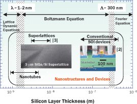
Figure 1. Regime map for phonon transport in ultra-thin silicon layers. Mean free path Λ is a distance that
phonons travel on average before being scattered by other phonons. If the dimension of the silicon layer is
smaller than Λ, the BTE should be used for heat transfer analysis of the thin film. The dominant phonon
wavelength, λ, at room temperature, is on the order of 2-3 nm. Analogous phonon wave simulations should
be performed for devices with thicknesses comparable to λ.

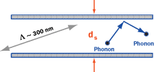
Figure 2. Phonon-boundary scattering is responsible for a large reduction in the thermal conductivity of a
thin silicon layer where the thickness of the film, ds , is comparable to or smaller than the phonon mean
free path, Λ.
Figure 1 compares the dimensions of several nanostructures (e.g., an SOI device and a superlattice structure) with the dominant phonon mean free path (MFP) and wavelength at room temperature. This graph also provides a general guideline for the appropriate treatment of phonon transport in nanostructures. Phonon transport can be predicted using the Boltzmann particle transport equations (BTE), which are required only when the scattering rates of electrons or phonons vary significantly within a distance comparable to their respective mean free paths.
The BTE simply takes care of the bin counting of the energy carrier particles of a given velocity and momentum, scattering in and out of a control volume at a point space and time. Analysis of the heat transfer in microelectronic devices, interconnects and nanostructures using the BTE is very cumbersome and complicated, even for simple geometries, and has been the topic of research and development in the field of micro- and nanoscale heat transfer for the past two decades [e.g., 4,5].
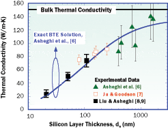
Detailed descriptions and analyses of the ballistic heat transfer in a semiconductor/metallic layer are beyond the scope of this article. However, the most prominent manifestation of ballistic heat transport in thin films would occur in the form of large reductions in thermal conductivity compared to the bulk values. Ballistic phonon transport in silicon films, or phonon-boundary scattering (see Figure 2), has been investigated through large measured reductions in the lateral thermal conductivity compared to the bulk value near room temperature [6-9] and is shown in Figure 3.

Figure 3. Room-temperature thermal conductivity data for
silicon film layers as a function of thickness.
The lateral thermal conductivity of the thin silicon layer decreases as the thickness of the film is reduced. Deviation of the thermal conductivity from the bulk value takes a sharp dive as the thickness of the film is reduced beyond 300 nm, which is the order of magnitude for the phonon mean free path in silicon at room temperature. For example, the thermal conductivity of the 20 nm thick silicon layer is nearly an order of magnitude smaller than the bulk value.
It should also be mentioned that the Fourier heat conduction equation cannot explain the thickness dependency of thermal conductivity in silicon. The impact of phonon-boundary scattering on the thermal conductivity of a thin silicon layer can be predicted (see Figure 3), using the BTE and the theory described by Asheghi et al. [6], such that it agrees very well with the experimental data [6-9].
Advanced Cu-dielectric interconnect technologies are central to the very large scale integration (VLSI) roadmap to improve the performance of integrated circuits. With shrinking device dimensions, interconnect resistance has become one of the major concerns in determining device performance. Typically, using copper instead of aluminum reduces interconnect electrical resistance by about 40%, resulting in better signal integrity, smaller propagation delays, lower power dissipation, and higher performance. In addition, the electro-migration properties of copper are better than those of aluminum.
It becomes increasingly important, therefore, to properly characterize and model the thermal behavior, and the associated reliability and failure mechanisms for very thin copper layers. It is clear that thermal characterization and modeling of multi-level interconnect systems, concurrently with those for packaging, are essential to address performance and reliability issues for future device and interconnect technologies.
In pure metals, heat is carried primarily by electrons. The electrical and thermal resistivities of copper layers are increased when the characteristic length scale of the interconnect wire (film thickness and/or width) or grain diameter (strongly processdependent) is comparable with or less than the electron MFP, which is about 50 nm. Once again, the prominent manifestation of the ballistic heat transport in a thin copper layer is in the form of large reductions in thermal conductivity compared to the bulk value.
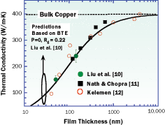
Figure 4 shows the measured lateral thermal conductivities of copper layers as a function of thickness near room temperature. The experimental data [10-12] agree very well with the predicted size effect based on BTE for the thermal conductivity of copper films [10], the prediction of which is strongly dependent on the specular reflection coefficients at the thin film, p, and grain, Rg, boundaries. The test vehicles of Liu et al. [10] with thin film thickness values of 50 nm and 144 nm were prepared using conventional microfabrication processes.

Figure 4. Comparison of predicted and experimental data for thin copper layers.
Clearly, the micro/nanoscale heat transfer effects in the silicon and copper interconnect layers of thin films have a huge impact on the thermal engineering of the deep sub-micron SOI, strained-Si transistors, and copper-dielectric network as well as on the thermal analyses of the micro- and nanoscale structures. In particular, the so-called size effect can reduce the thermal conductivity of a nanostructure by nearly an order of magnitude.
One way to roughly estimate the impact of the micro/nanoscale effect is to use the modified thermal conductivity values for thin silicon and copper layers in conventional thermal simulation tools that use the continuum theory or diffusion equation. However, one should be cautious that these tools can by no means capture the non-equilibrium energy transport in nanostructures and provide only an estimate for the effective thermal resistance of a given device.
At the same time, the temperature distribution and heat flux patterns in a non-equilibrium condition could be entirely different from those predicted by the Fourier heat conduction equation. It should also be mentioned that the proposed approach should be implemented with extra care and with a full understanding and mastery of sub-continuum heat transport effects and concepts.
The thermal boundary resistance at the interfaces of high thermal conductivity materials, such as copper-silicon (metaldielectric) and silicon-germanium (dielectric-dielectric), are often the dominant thermal resistance in the heat conduction path in micro- and nanoscale devices and structures, and should be carefully accounted for in the estimation of the total thermal resistance of a given device. For example, the contact resistance between metaldielectric layers can vary between 5 x 10⁻⁹ and 5 x 10⁻⁷ m2K/W, depending on the processing conditions and quality of the interface [13], which are comparable to those of 1 and 100 μm thick silicon layers, respectively.
The thermal contact resistance between dielectrics, such as Si and Ge in SiGe superlattices (for a thermoelectric application), could be as small as 5 x 10-11 to 5 x 10⁻¹⁰ m2K/W [14]; however, the total thermal resistance of the SiGe superlattice consists of hundreds of SiGe bi-layers and thus could be relatively large. Phonon transport at the interface of single crystalline dielectrics layers is one of the most exciting and heavily studied topics in the field of micro- and nanoscale heat transfer [e.g., 14-16].
In the ultra-fast laser heating processes at time scales of 10-15 to 10-12 seconds, as well as high speed transistors switching at timescales in the order of 10-11, the temperatures of the electron and phonon systems are not in equilibrium and may differ by orders of magnitude. Even after the phonon and electron reach equilibrium, the energy carried away by phonons can travel only to 10-100 nanometers; therefore, the temperature of the transistor can easily rise to several times its designed reliability limit.
Under these circumstances, regardless of the cooling solution at the packaging level, a catastrophic failure at the device level can occur, because the impact of the rapid temperature rise is limited to the device and its vicinity. As a result, while the package level cooling solutions can reduce the quasi steady-state/average temperature across a microprocessor or at length scales in the order of one millimeter, it has very little impact at micro/nanoscales. Basically, there is no practical way to reduce the temperature at the device and interconnect level by means of a cooling device or solution; therefore, the options for thermal engineering of these devices are very limited.
However, intelligent electro-thermal design along with careful floor planning at the device level can largely reduce the temperature rise within a device. This means that the role of the thermal engineer is to properly anticipate – perhaps in full collaboration with electrical engineers – and prevent the problem at the early stages and at the device level, rather than to pass the problem to the package-level thermal engineers.
References
- Borkar, S., “Design Challenges of Technology Scaling,” IEEE Micro, Vol. 19, 1999, pp. 23-29.
- Geppert, L., “Solid state [semiconductors. 1999 technology analysis and forecast],” Spectrum, IEEE, Vol. 36, 1999, pp. 52-56.
- Zeng, G., Fan, X., LaBounty, C., Croke, E., Zhang, Y., Christofferson, J., Vashaee, D., Shakouri, A., Bowers, J.E., “Cooling Power Density of SiGe/Si Superlattice Micro Refrigerators,” Materials Research Society Fall Meeting 2003, Proceedings Vol. 793, paper S2.2, December 2003, Boston, MA.
- Majumdar, A., “Microscale Heat Conduction in Dielectric Thin Films,” Journal of Heat Transfer, Vol. 115, 1993, pp.7-16.
- Chen, G., “Ballistic-Diffusive Heat-Conduction Equations,” Physical Review Letters, Vol. 86, 2001, pp. 2297-2300.
- Asheghi, M., Touzelbaev, M.N., Goodson, K.E., Leung, Y.K., and Wong, S.S., “Temperature Dependent Thermal Conductivity of Single-Crystal Silicon Layers in SOI Substrates,” ASME Journal of Heat Transfer, Vol.120, 1998, pp. 30-33.
- Ju, Y. S., and Goodson, K. E., “Phonon Scattering in Silicon Films with Thickness of Order 100 nm,” Applied Physics Letters, Vol. 74, 1999, pp. 3005-3007.
- Liu, W. and Asheghi, M., “Phonon-Boundary Scattering in Ultra Thin Single-Crystal Silicon Layers,” Applied Physics Letters, Vol. 84, 2004, pp. 3819-3821.
- Liu, W. and Asheghi, M., “Thermal Conductivity of Ultra-Thin Single Crystal Silicon Layers,” Journal of Heat Transfer, Vol. 128, 2005, pp. 75-83.
- Liu, W., Yang,Y., and Asheghi, M., “Thermal and Electrical Characterization and Modeling of Thin Copper Layers,” Intersociety Conference on Thermal and Thermomechanical Phenomena in Electronic Systems (Itherm), San Diego, California, May 2006.
- Nath, P., and Chopra, K. L., “Thermal Conductivity of Copper Films,” Thin Solid Films, Vol. 20, 1974, pp. 53-62.
- Kelemen, P. G., “Pulse Method for the Measurement of the Thermal Conductivity of Thin Films,” Thin Solid Films, Vol. 36, 1976, pp. 199-203.
- Ruxandra M., Costescu, M., Wall, A., and Cahill, D.G., “Thermal Conductance of Epitaxial Interfaces,” Physical Review B, Vol. 67, 2003, 054302.
- Chen, G. and Shakouri, A., “Heat Transfer in Nanostructures for Solid-State Energy Conversion,” Journal of Heat Transfer, Vol. 124, 2002, pp. 242-252.
- Vashaee, D., and Shakouri, A., “Electronic and Thermoelectric Transport in Semiconductor and Metallic Superlattices,” Journal of Applied Physics, Vol. 95, 2004, pp. 1233-1245.
- Vashaee, D., and Shakouri, A., “Nonequilibrium Electrons and Phonons in thin film thermionic coolers,” Microscale Thermophysical Engineering, vol. 8, pp. 91-100.


