Bernie Siegal
Thermal Engineering Associates, Inc.
Introduction
One of the key power generation technologies in the current “green” revolution is the solar photovoltaic cell (SPVC). This unit directly converts solar energy into useful amounts of electrical energy in an increasingly economically-efficient manner. But the SPVC is not a new device – in semiconductor device terms, it is just a diode, and has been around for many decades. The newness of the SPVC lies in the increased energy conversion efficiencies and the ability of industry to find ways to lower the manufacturing and implementation costs while improving the performance and reliability. A key element in the performance and reliability improvements has centered on better control of the cell’s junction temperature.
Even though a thermal measurement standard specific to the SPVC does not currently exist, the fact that it is “just a diode” provides implementation of existing measurement standards for both junction temperature and thermal resistance. This measurement capability is necessary for gauging the effectiveness of manufacturing and implementation techniques intended to better control junction temperature.
SPVC Types
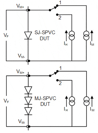
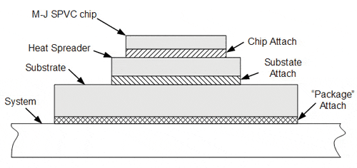
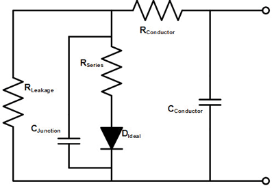
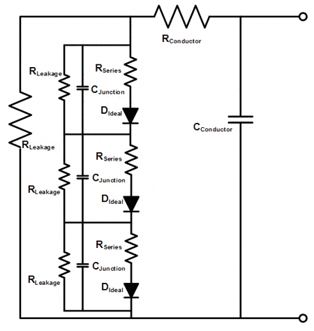
There are several different technologies that can be used to directly convert solar energy into electricity [1]. However, the discussion herein will be limited to two of the most common semiconductor junction technologies – the Single Junction SPVC (SJ-SPVC) and the Multi-Junction SPVC (MJ-SPVC). The SJ-SPVC devices are made from silicon or germanium and are usually made by the normal semiconductor manufacturing process. This results in chips – which may be as large as 200 mm square for silicon chips and up to 100 mm square for germanium versions. These chips are mounted in the normal semiconductor fashion – either with eutectic, soft solder, or epoxy – to a mounting surface that acts as the “package.” The Multi-Junction SPVC (MJ-SPVC) devices are actually three diodes in series, all implemented in one chip. The chip material is usually a III-V compound with three different sets of junction materials. Each junction is “tuned” in for a different solar energy wavelength range using the bandgap associated with the different material combinations. The electrical equivalent circuits for these two types are shown in Figures 1 and 2, respectively.
The leakage and series resistances, junction capacitance, and ideal diode shown in the SJ-SPVC equivalent circuit are the circuit elements usually shown for just about any diode. The conductor resistance and capacitance elements are also common to diodes in general but can usually be neglected in most cases. But these cannot be neglected in the SPVC case because the conductor is relatively long, typically traveling across the whole cell, and because of the high currents involved. For reasons discussed below, both of these elements impact the measurement of SJ-SPVC thermal performance.
The MJ-SPVC equivalent circuit for these devices is similar to that shown in Figure 1, except that each junction has its own RLeakage, RSeries, CJunction, and DIdeal; and the three junctions are all connected in series. Because the three junctions are made from different materials, the circuit elements for each series diode will be different from the other junctions in the stack. It is important to note that even though there are three distinct diodes in the stack, direct access to an individual diode is not present.
Performance Limiters
A key measure of SPVC performance is the cell’s ability to convert incident solar energy (i.e., light) into electrical energy. Commercially available SPVC modules currently offer conversion efficiencies in the range of 12% for SJ and 28% for MJ units. The maximum theoretical conversion efficiency (about 30% and 68%, for SJ and MJ types, respectively) is determined by the Shockley–Queisser limit that deals with the amount of photon energy that can actually be converted into electrical energy [2]. The theoretical limit is not reachable because of the following key performance limiters:
Semiconductor Processing Limitations: The object of solar photovoltaic cells is to collect as
much solar energy (i.e., light) as possible and convert that energy into electrical energy.
By definition then, SPVCs are made as large as reasonably possible for both single and multi-junction cells. The large junction areas for either type make each susceptible to wafer fabrication defects. Defects that may not render the cell useless but will reduce the conversion efficiency and potentially cause hot spots on the cell.
Conductor Series Resistance: The backside conductor usually is not a problem because of its large area and it is out of the light path. However, the top conductor series resistance affects performance in two ways. First, a portion of the electrical energy generated by the photovoltaic diode is converted into Joule heating. This increases localized junction temperature and degrades the cell output. Second, the voltage dropped across the conductor reduces the output voltage, and hence the power, available as the cell’s output, thus reducing the cell conversion efficiency even further.
Conductor Shadowing: The natural tendency, based on the conductor series resistance issues above, is to increase the size of the conductor or use more conductors to reduce the resistance. However, any increase in the width of the conductor or the number of conductors will increase the shadowing of the cell’s active area, which will in turn reduce the conversion efficiency as well. Increasing the conductor thickness does help but also introduces manufacturing issues.
Junction Temperature: Like all diode devices, the junction forward voltage under given current flow decreases with junction temperature. As shown in Figure 3, the SPVC has a near constant current output up to some voltage that is temperature dependent. The higher this voltage for a given current, the higher the power output of the cell. Thus, maintaining the lowest possible junction temperature maximizes the power conversion efficiency and the electrical energy output. Although this generic I-V curve shown is for a SJ-SPVC, the temperature dependency for a MJ-SPVC is very similar, with the voltages about three times higher.
Three out of four key limiters directly impact overall SPVC performance through temperature effects, thus making the lowest possible junction temperature maintenance paramount.

Incident Power
SPVCs are unique in the diode family when the source of the power dissipation is considered. Most diodes have internal power dissipation resulting from the application of external energy to the device. The SPVC has little internally generated power dissipation but a lot of incident externally-sourced power dissipation. However, some of the incident power is converted to electrical power out, thus reducing the thermal impact.
One sun, a term used in the solar photovoltaic industry to describe the incident power, is approximately 1,000 W/m2, or 0.1 W/cm2 [3, 4]. A concentration ratio of 100 suns, obtainable by using optical lens [5] or mirrors [6], would provide a power
density of 100,000 W/m2 or 10 W/cm2.
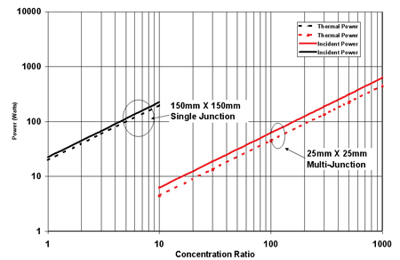
Applying these values to SPVC power dissipation considerations produces interesting results. The SJ-SPVC typically operates with 1 to 10 times the incident solar power, while the MJ-SPVC operates with much higher concentration values – 50 to 1000 times. Figure 4 shows the magnitude of the incident power for concentration ratios and for different cells.
For example, consider a 150 mm X 150 mm silicon SJ-SPVC operating at one sun would have about 22.5 W incident and about 19.8 W in thermal power assuming 12% conversion efficiency. Similarly, a 25 mm X 25 mm MJ-SPVC operating at 100 suns would have about 62.5 W incident and about 45 W in thermal power assuming 28% conversion efficiency. Power densities for these cases are 0.088 W/cm2 and 7.2 W/cm2, respectively. This thermal power is what the SPVC system, consisting of the cell and its mounting environment, has to properly dissipate to keep the cell junction temperature in the desired operating range.
