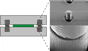
The researchers have demonstrated that two chips can be vertically interconnected with carbon nanotubes by through-silicon via interconnects, and that the chips can be bonded. They have also demonstrated that the same method can be used for electrical interconnection between the chip and the package.
Two chips have interconnects that are filled with thousands of carbon nanotubes. The chips are then bonded with adhesive so that the carbon nanotubes are directly contacted.
For the method to be transferred to industrial production, manufacturing temperature needs to be reduced to a maximum of 450 degrees. This is a great challenge since carbon nanotubes are currently “grown” at a minimum of 700 degrees.
If successful, entirely new possibilities will arise for future shrinking of electronics – not least in terms of improved performance. The three dimensional integration using through-silicon vias provides significantly quicker signal transfers than traditional integration where chips are placed next to each other. Furthermore, through-silicon vias with carbon nanotubes provide less expensive production compared to the current technology that uses copper interconnects.


